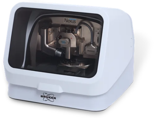
Dimension Nexus™ provides an optimal combination of data quality, experimental flexibility, and ease of use within a compact system. It incorporates the advanced features of the Bruker NanoScope® 6 controller, PeakForce Tapping® technology, and ScanAsyst® Plus, delivering greater functionality than competing systems in its category.
Suitable for both routine and specialized experiments, and easily upgradable on-site, Dimension Nexus serves as an excellent entry-level system as well as a valuable addition to any established AFM laboratory.
Dimension Nexus: A New High-Performance Standard for Cost-Effective AFMs
Video Credit: Bruker Nano Surfaces and Metrology
- Best-in-class performance: Facilitates imaging from atomic to molecular resolution
- Ultimate versatility and value: Offers a wide array of AFM modes
- Programmable motorized stage: Enhances productivity for results ready for publication
Features
Provides Core Performance and Value in Every Scan
Nexus reliably produces results that are highly accurate, reproducible, and ready for publication across a diverse array of sample types in both research and industrial applications.
Ensuring High Performance
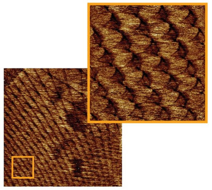
High-resolution topography images of a van der Waals heterostructure showing a moiré superlattice. Images collected in torsional resonance dynamic force microscopy (TR-DFM) with a FESPA probe. Scan sizes 1 × 1 µm and 200 × 200 nm (orange box). Image Credit: Bruker Nano Surfaces and Metrology
At the heart of this system's superior capabilities lies its distinctive integration of advanced hardware, software, and accessories, which include:
- Comprehensive range of PeakForce Tapping modes designed for the highest resolution imaging and quantitative mapping of mechanical, electrical, and chemical properties across a diverse array of samples.
- State-of-the-art NanoScope 6 controller featuring minimal noise, maximum speeds, and exceptional versatility, providing unmatched capabilities and user-friendliness.
- XYZ closed-loop scanner with a drift-compensated bridge structure and an integrated granite base, ensuring optimal performance for small samples in an open-access, large-sample AFM environment.
- The most extensive selection of specialized AFM Probes is tailored for specific modes and sample types.
Guaranteeing Stability
![[Top] Start and end of an array of 360 trenches with an overall scan size of 90 × 2 µm (16384 × 16 px) in PeakForce Tapping with an SAA-HPI probe. Critical dimension analysis showed no scanner artifacts or tip degradation over the full range. [Bottom] Trench-to-trench pitch measurements across all 360 trenches, showing near-zero deviation over the entire scan range.](https://www.azom.com/images/equipments/EquipmentImage_9790_1777884134110416.png)
[Top] Start and end of an array of 360 trenches with an overall scan size of 90 × 2 µm (16384 × 16 px) in PeakForce Tapping with an SAA-HPI probe. Critical dimension analysis showed no scanner artifacts or tip degradation over the full range.
[Bottom] Trench-to-trench pitch measurements across all 360 trenches, showing near-zero deviation over the entire scan range. Image Credit: Bruker Nano Surfaces and Metrology
When imaging for extended durations, Dimension Nexus demonstrates negligible drift, and across lengthy scan lengths, the system reveals no scanner artifacts or tip degradation.
Delivers Outstanding Value and Ease of Use
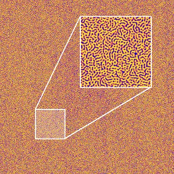
Phase image of a styrene butadiene block copolymer (SBC), collected in TappingMode with an RTESPA probe. Full scan size is 5 × 5 µm, (2560 × 2560 px). Inset is a digital zoom showcasing the data density and level of detail retained. Image Credit: Bruker Nano Surfaces and Metrology
Nexus offers unique benefits for researchers operating early-stage laboratories or those intending to enhance the AFM research in the future:
- The base setup - which includes a programmable stage for high-throughput, multi-site measurements - quickly provides high-quality data that is suitable for standard applications.
- Individuals with varied experience levels can achieve dependable results, thanks to user-friendly features, including simplified sample/probe setup, ScanAsyst self-optimizing imaging, and sophisticated data analysis software.
- A wide range of upgrade options, including distinctive operating modes, dependable environmental control, and robust software integrations, guarantees that the system can evolve alongside the research.
Offers Future Versatility and Customization
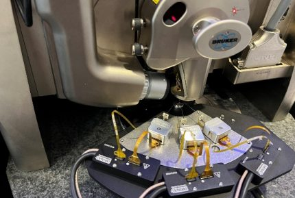
Microprobers integrated with Dimension Nexus for electrical characterization of nanodevices. Image Credit: Bruker Nano Surfaces and Metrology
Dimension Nexus is upgradable and offers open access to enable users to customize experiments. The probe-sample junction is physically accessible, making it possible to attach electrical connections and various custom accessories.
The NanoScope 6 controller features an open hardware and software platform, equipped with front-panel BNC connectors, options for scripting software, and straightforward data import capabilities to Python for tailored analyses.
Applications
Enables Full Range of Applications
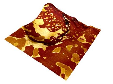
PeakForce quantitative nanomechanics (PeakForce QNM®) can be used to map distribution of components in polymer blends. PS-PMMA-PVC sample courtesy of U. Mons. Scan size 5 × 5 µm, RTESPA-150 probe. Image Credit: Bruker Nano Surfaces and Metrology
Nexus is equipped with a 150 mm open-access programmable stage and is compatible with the majority of Bruker's 50+ modes, including full PeakForce Tapping capabilities, fluid imaging, environmental control, and more.
The equipment provides cost-effective AFM excellence suitable for a diverse array of applications and experiments, such as:
- Manipulating and characterizing the electrical properties of DNA nanowires for nanoelectronic devices
- Conducting in situ and operando studies of the local electrochemical activity of lithium-ion batteries
- Correlating the structural and ferroelectric properties of perovskites in photovoltaics
- Characterizing graphene, moiré superlattices, and other 2D materials at the nanoscale
- Quantifying the nanoscale surface roughness of semiconductor thin films and substrates
- Mapping the nanomechanical properties of polymers and composite materials
Specifications
Dimension Nexus Select Specifications
Source: Bruker Nano Surfaces and Metrology
| |
|
| X-Y Scan Range |
90 μm x 90 μm typical, 85 μm minimum |
| Z Range |
10 μm typical in imaging and force curve modes, 9.5 μm minimum |
| Sample Size/Holder |
150 mm vacuum chuck for samples, ≤150 mm diameter, ≤15 mm thick |
| Motorized Positioning (XY Stage) |
150 mm x 150 mm inspectable area; 6 μm repeatability, bidirectional; programmable for multi-site measurements |
| Microscope Optics |
5 MP digital camera; 180 μm to 1465 μm viewing area; digital zoom and motorized focus |
| Certification |
CE |
What Dimension AFM is Right?
Bruker offers a wide range of high-quality AFM systems, with the Dimension family featuring industry-leading imaging and characterization technologies developed through decades of experience and close collaboration with researchers.
At the top tier, the Dimension Icon establishes the benchmark for commercial AFM performance. Now, Dimension Nexus is added to the portfolio, providing strong value and capabilities in a more cost-effective system.
The Dimension Nexus: Best-in-class general-purpose AFM. Image Credit: Bruker Nano Surfaces and Metrology
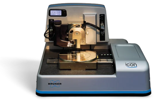
Dimension Icon: Gold standard for advanced large-sample AFMs. Image Credit: Bruker Nano Surfaces and Metrology
Key Features and Specs
Source: Bruker Nano Surfaces and Metrology
| |
Dimension Nexus |
Dimension Icon |
| Sample Size (XY) |
150 mm |
300 mm |
| Motorized Stage Range |
150 mm x 150 mm |
150 mm x 180 mm |
| Small & Multi-Sample Compatibility |
Yes |
Yes |
| Sample Flexibility |
Tip Scanner |
Tip Scanner |
| XY-Scan Range |
90 µm x 90 µm |
90 µm x 90 µm |
| Z-Range |
10 µm |
10 µm |
| System Footprint (W x L) |
24" x 32" (plus customer desk/workstation) |
47" x 94" (including integrated workstation) |
| Controller |
NanoScope 6 |
NanoScope 6 |
| Programmable Measurements |
Yes |
Yes |
| Automated Metrology Recipes |
No |
Yes |
| Open-Access Platform |
High degree of flexibility for customization |
Maximum flexibility for customization |
Measurement Capabilities
Source: Bruker Nano Surfaces and Metrology
| |
Dimension Nexus |
Dimension Icon |
| High-Resolution Imaging |
Atomic lattice resolution |
Atomic defect resolution |
| High-Speed Imaging |
Fast Tapping |
FastScan dedicated high-speed AFM; Fast Tapping |
| PeakForce Tapping |
Yes |
Yes |
| ScanAsyst (Self-Optimizing Imaging) |
Yes |
Yes |
| PeakForce Tapping Derivative Modes |
Yes |
Yes |
| Chemical Identification Capability |
No |
IconIR upgradable |
| Hyperspectral Imaging |
DataCube |
DataCube |
| Other Modes & Options |
Wide range to address majority of applications |
Complete range for industry-leading application coverage |
Software
Powered by the NanoScope 6 AFM Controller
With enhanced speeds, reduced noise levels, and increased flexibility in AFM modes, the NanoScope 6 controller enables users to leverage the capabilities of the advanced Dimension and MultiMode AFM systems. This newest generation of controllers offers unmatched accuracy, precision, and versatility for nanoscale surface measurements across all applications.
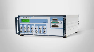
NanoScope 6 AFM controller. Leading-edge AFM controller built on an innovative high-speed, low-noise architecture for delivering unprecedented measurement performance. Image Credit: Bruker Nano Surfaces and Metrology
NanoScope 6 Uniquely Enables Bruker AFMs to:
- Employ a wider variety of imaging modes compared to competing systems, showcasing unique and advanced AFM modes that require detailed control and analysis
- Gather precise, quantitative data for measurements of nanoelectrical and nanomechanical properties across all applications
- Refine and tailor scanning parameters to satisfy even the most rigorous demands of research and industrial measurement standards
- Ensure maximum user-friendliness with Bruker’s proprietary ScanAsyst® Plus self-optimizing imaging software, which incorporates advanced intelligent algorithms and innovative smart functionality