When atoms and/or electrons are constrained to an atomically flat plane, 2D materials exhibit properties not typically observed in their 3D counterpart, including excellent strength and conductivity. These properties open new avenues for the development of groundbreaking electronic devices while advancing the functionality of silicon-based chips.
For functional customization, 2D materials can be stacked to create heterostructures.1 High surface area promotes chemical reactivity, advantageous for catalysis, chemical/biological sensing, energy storage, and drug delivery.
Atomic force microscopy (AFM) can be a key component in the characterization of 2D materials, as it provides nanoscale, high-resolution topographical, mechanical, and electrical property mapping.
The combination of infrared spectroscopy with AFM enables localized chemical identification with nanometer-scale spatial mapping, a technique referred to as photothermal AFM-IR (AFM-IR).
This combination probes both material structure and chemistry, enabling in-depth studies of sophisticated 2D material systems. This article discusses how AFM-IR is compatible with and can be used alongside scattering-type scanning near-field optical microscopy (-SNOM).
This is achieved by presenting FTIR-correlated spectra and chemical maps at ∼10 nm resolution, including direct absorption imaging of hBN phonon polaritons and contrast specific to layer stacking in graphene heterostructures.
From s-NOM to Photothermal AFM-IR
s-SNOM is a verified AFM-based measurement approach for the acquisition of nanoscale chemical and optical properties. This is achieved by using the AFM tip as a local antenna and focusing the incident light on it. In s-SNOM, an interferometer identifies scattered light being transmitted over the local complex refractive index (n, k).
Complete access to the optical refractive index and absorption coefficient is enabled by extracted optical constants that correspond to chemical composition and optical resonances. The light-matter interaction, which is localized beneath the AFM tip, allows spatial resolution of less than 10 nm.
Widespread use of s-SNOM has been recognized across the field of research on surface polaritons, which arise from the interaction between light (photons) and the collective oscillations of charged particles, including electrons (plasmons) in conductors or the vibrational modes of atoms (phonons) in dielectrics.
Visualization of the real space of confined surface polaritons on 2D materials is conducted using -SNOM, which reveals their wavelengths, propagation lengths, and interference patterns. Photothermal AFM-IR is considered a newer method in 2D material characterization in comparison to s-SNOM: the schematic diagram in Figure 1 demonstrates the difference between the two.
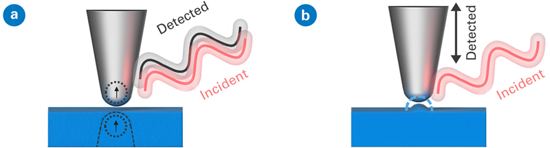
Figure 1. Representations of the operation of (a) s-SNOM and (b) AFM-IR. Image Credit: Bruker Nano Surfaces and Metrology
In AFM-IR, tunable IR light is focused and pulsed onto the sample at the AFM tip location. When the IR wavelength matches the absorption band of the material, rapid local thermal expansion stimulates cantilever oscillations, which the AFM is able to measure.
The signal from photothermal AFM-IR directly measures sample absorption, yielding spectra that correspond to those obtained with traditional Fourier-transform infrared (FTIR) in transmission mode.
Pre-2015 studies evaluating the suitability of AFM-IR for the characterization of 2D materials were hindered by weak signals due to their low thermal expansion coefficient and narrow dimensions. Breakthroughs in detection sensitivity (down to monolayers/single molecules) and spatial resolution (<5 nm) make AFM-IR an effective tool for the nanoscale characterization of 2D materials.
AFM-IR offers many advantages over s-SNOM, including faster measurements, simpler interpretation, and displacement-based detection rather than basic optical methods, giving it a strong position in the rapidly advancing field of 2D materials research.
Previous Studies of 2D Materials with AFM-IR
AFM-IR as a Complement to s-SNOM
AFM-IR has been frequently used to support s-SNOM for the analysis of 2D materials in numerous studies, including plasmon polariton in graphene monolayer, phonon polariton in hBN and MoO3, and circular dichroism in 2D planar-chiral metamaterials.2-6
For graphene monolayers, both Tapping AFM-IR and s-SNOM reveal SPP interference fringes with full intensity at the graphene wedge periphery as displayed in the IR images recorded at 930 cm-1.
This agreement confirms fringe spacing and intensity, showing a correlation between the s-SNOM SPP mode and AFM-IR tapping.2 Phonon polaritons have similarly been observed and analyzed in flakes as thin as 4 nm in hBN.4
AFM-IR for Unique Property Characterization
AFM-IR has the capacity to record properties more difficult to measure, unlike techniques that are purely dependent on optical near-field imaging. AFM-IR can measure heat dissipation mechanisms in graphene, non-radiative states in hBN, photothermal effects in thicker hBN, functionalized graphene, and MXene/graphene oxide hybrids:
- AFM-IR spectra from a graphene flake and SiO2 substrate demonstrate sturdy hybridization within graphene plasmon and SiO2 phonon modes in the 900–1200 cm-1 range, consistent with the photothermal expansion signal.2
- For hBN frustums (256 nm thick) with fluctuating aspect ratios, AFM-IR spectra displayed a diverse range of peaks, including some strong enough to reach over 1550 cm-1, among which were those allocated to non-radiative higher order modes, with a broad selection of angular and radial momenta.3
- AFM-IR has also opened up the possibility for large photothermal expansion in nanostructured hBN associated with the height-to-width aspect ratio. This effect is related to the large anisotropy of the thermal expansion coefficients of hBN in addition to the applied nanostructuring.7
- There have been a number of studies on functionalized graphene materials. One study in particular shows that three different functional groups were covalently bonded to the graphene basal plane in a dense and unambiguous pattern.8-11
- The distinctions are clear to see in the AFM-IR results, shown in Figure 2, showing the differences between the patterned regions and the underlying graphene layer, as well as any variations among the various functionalized patterns.10
- AFM-IR has also found utility for the study of hydrogen bonds that are produced between MXene and graphene oxide nanosheets, which evidently increased nanocomposite stability by lowering the overall energy of the system.12
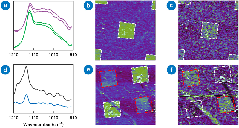
Figure 2. AFM-IR spectra and images of graphene with covalent chemical patterning. (a) Spectra on (purple) and off (green) pattern for sample 1. (b) and (c) ratio IR image of 970:1100 cm-1 and 1730:1100 cm-1 of sample 1. (d) AFM-IR spectra on two different patterns for sample 2. (e) and (f) ratio IR image of 970:1100 cm-1 and 1730:1100 cm-1 of sample 2. Scan size: 20x20 μm. Sample courtesy Steven De Feyter (KU Leuven). Image Credit: Bruker Nano Surfaces and Metrology
Case Studies
AFM-IR Study of Phonon Polaritons in hBN
Greater spatial confinement can be observed in the SPPs and phonon polaritons (PhPs) of 2D materials, granting opportunities for the development of amplified light–matter interaction, improved super lenses, better subwavelength metamaterials, and new groundbreaking photonic devices.
PhP loss is reduced when observed in hBN in contrast to graphene’s SPPs, encouraging extended polariton lifetimes and propagation lengths, especially in isotopically enriched or suspended hBN.
Tapping AFM-IR measurements for a thin hBN flake on a Si/SiO2 substrate over the upper Reststrahlen band (1360–1600 cm-1) clearly show that the phonon polaritons correlate with the stimulated wavelengths. Results agree with the theory and prior s-SNOM study reviews, thereby validating AFM-IR suitability for quantitative phonon polariton studies.13
Figure 3 shows the topographic and Tapping IR data for a flat 75 nm-thick hBN flake on Si/SiO2. The images were captured using the Dimension IconIR® system, with a specific set of Tapping IR images taken from 1400 to 1580 cm-1 in 20 cm-1 intervals, with three representative images shown at 1480, 1520, and 1560 cm-1. The fringe patterns, generated by the interference of surface polariton waves, were clearly observed across each of the IR images.
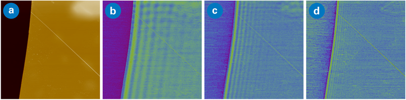
Figure 3. Topography and IR absorption images of a 75 nm thick hBN flake on Si/SiO2. (a) Topography and (b-d) IR images at 1480, 1520, and 1560 cm-1, obtained with Tapping AFM-IR. Scan size: 10x10 μm. Image Credit: Bruker Nano Surfaces and Metrology
Using the theoretical models explained by Equation 1 in Dai et al., alongside the parameters for hBN in Table S4 of Giles et al., it is possible to determine the predicted momentum of hBN polaritons in response to excitation wavelengths in the upper Reststrahlen band. The general trend refers to the experimental data, while the dashed curve represents the theoretical results.13,14
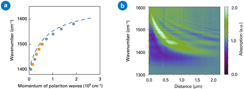
Figure 4. (a) Comparison of measured momentum of the polariton waves (points) with theoretical values (dashed curve). The gray circles and orange squares are results measured on IconIR and nanoIR3 instruments, respectively. (b) Spatio-spectral imaging of phonon polaritons in hBN. Image Credit: Bruker Nano Surfaces and Metrology
An array of 210 spectra were captured via Tapping AFM-IR over the hBN/SiO2 boundary and into the hBN flake, at a spacing of 12.5 nm and with the array situated at 90 ° to the edge of the hBN.
Figure 4b plots the IR signal intensity of the normalized spectra as a function of distance from the hBN/SiO2 boundary. The spatio-spectral image exhibits polaritonic features that match those observed in s-SNOM imaging, validating the suitability of AFM-IR for the study of phonon polaritons in hBN.13
AFM-IR Study of Stacking Order in Multilayer Graphene
Multilayer graphene may, at times, demonstrate differing orders of stacking, such as Bernal (ABAB), rhombohedral (ABCA or ACBA), or intermediate (ABCB). Stacking order has a major impact on the electronic properties of the material. This makes it all the more important to verify the stacking order for device fabrication.
Conventional techniques (e.g., angle-resolved photoemission, infrared spectroscopy, and Raman spectroscopy) are not always compatible with identification techniques due to low resolution. At times, they may be able to deliver only relative contrast, yet this hinders the characterization of stacking orders in multilayer graphene. Working with Prof. Andrea Young’s group at the Department of Physics, UC Santa Barbara, photothermal AFM-IR was combined with scanning microwave impedance microscopy (sMIM) to overcome any limitations.15
Tapping IR imaging revealed clear distinctions between domains in a trilayer and tetralayer graphene sample (Figure 5). Domains with differences in the stacking orders were verified using cross-validation of AFM-IR, sMIM, and coherent Raman. These domains reveal individual electrical properties, which were confirmed by sMIM. AFM-IR spectra captured at three different domains revealed further distinctions in specific IR spectral fingerprints, including the characteristic resonance at 1576 cm-1.
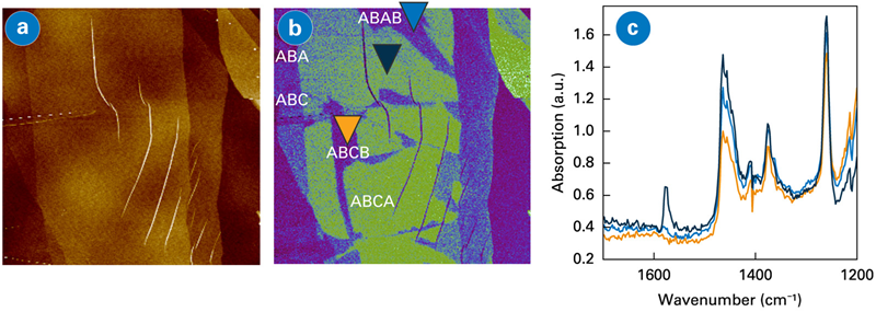
Figure 5. (a) Topography and (b) Tapping AFM-IR images at 1576 cm-1 of a multilayer graphene sample on SiO2. (c) Tapping IR spectra collected at three locations with markers of the same colors in the IR image. Scan size: 30x30 μm. Sample courtesy: Andrea Young, UCSB. Image Credit: Bruker Nano Surfaces and Metrology
What’s more, the narrow domain walls separating various regions of multilayer graphene were exposed via the high-resolution AFM-IR imaging displays. The domain walls correspond to the shear strain across the graphene flake during domain transitions.
The topographic and IR absorption data are displayed in a series of images (Figure 6) at 1576, 1260, and 1128 cm-1, with several stacking orders identified. A clear domain wall separating two rhombohedral (ABCA and ACBA) is visible in the IR images at 1260 and 1128 cm-1, with a detailed analysis showing the domain wall width at the 10 nm scale.
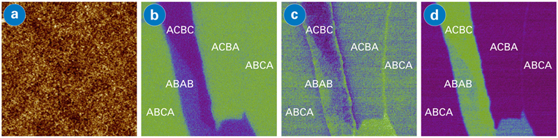
Figure 6. (a) Topography and (b-d) IR images at 1576, 1260, and 1128 cm-1, with (c) and (d) showing domain walls between ACBA and ABCA. Scan size: 3.5x3.5 μm. Sample courtesy: Andrea Young, UCSB. Image Credit: Bruker Nano Surfaces and Metrology
AFM-IR is perfect for visualizing the graphene layers found in van der Waals heterostructures. Figure 7 shows topographic and IR data from trilayer flakes, highlighting both rhombohedral (ABC) and Bernal (ABA) stacking regions, beneath 5-10 nm layers of hBN.
A number of bright dots exposed in the topography image resulted from trapped air bubbles between the graphene trilayer and outer hBN layer; otherwise, the graphene flakes exhibited a smooth profile.
The IR images reveal more detail, and it can be seen that the signal is boosted at 1576 cm-1 for the ABC trilayer in contrast to the ABA trilayer. This correlates with the contrast for the encapsulated graphene trilayer in Figure 5. Inverse contrast was observed in the IR image at 1128 cm-1 between the ABC and ABA trilayers.
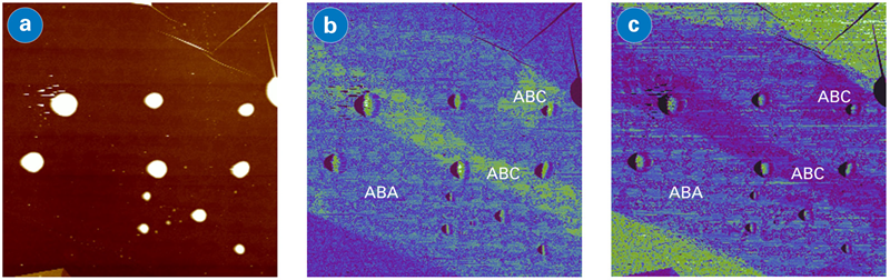
Figure 7. Subsurface imaging of trilayer graphene encapsulated by hBN. (a) Topography and (b,c) IR images at 1576 and 1128 cm-1. Scan size: 20x20 μm. Sample courtesy: Andrea Young, UCSB. Image Credit: Bruker Nano Surfaces and Metrology
These results confirm the suitability of AFM-IR, when paired with correlative techniques (such as sMIM in this study), for the study of graphene stacking orders, in addition to its capacity to identify nanoscale walls across various domains and capture buried graphene layers within van der Waals heterostructures.
AFM-IR Correlates Structure and Chemistry in 2D Materials at the Nanoscale
This work demonstrates that photothermal AFM-IR is a powerful technique for characterizing 2D materials, including those on plasmon-polariton modes in graphene and phonon-polariton modes in hBN.
While AFM-IR complements s-SNOM, it also provides a number of distinct benefits. Unlike s-SNOM, AFM-IR can directly probe non-radiative “dark” states, heat transfer functionality, and the chemistry of functionalized graphene.
With its sophisticated detection sensitivity, spatial resolution, measurement speed, and user-friendliness, AFM-IR is well-positioned to meet the growing demand for a more in-depth understanding of 2D materials while advancing the search for new materials.
References and Further Reading
- Pham, P.V., et al. (2022). 2D Heterostructures for Ubiquitous Electronics and Optoelectronics: Principles, Opportunities, and Challenges. Chemical Reviews, 122(6), pp.6514–6613. DOI: 10.1021/acs.chemrev.1c00735. https://pubs.acs.org/doi/10.1021/acs.chemrev.1c00735.
- Menges, F., et al. (2021). Substrate-enhanced photothermal nano-imaging of surface polaritons in monolayer graphene. APL Photonics, (online) 6(4). DOI: 10.1063/5.0044738. https://pubs.aip.org/aip/app/article/6/4/041301/123665/Substrate-enhanced-photothermal-nano-imaging-of.
- Brown, L.V., et al. (2018). Nanoscale Mapping and Spectroscopy of Nonradiative Hyperbolic Modes in Hexagonal Boron Nitride Nanostructures. Nano Letters, 18(3), pp.1628–1636. DOI: 10.1021/acs.nanolett.7b04476. https://pubs.acs.org/doi/10.1021/acs.nanolett.7b04476.
- Ciano, C. et al. (2018) 'Observation of phonon-polaritons in thin flakes of hexagonal boron nitride on gold,' Applied Physics Letters, 112(15). DOI: 10.1063/1.5024518. https://pubs.aip.org/aip/apl/article-abstract/112/15/153101/35592/Observation-of-phonon-polaritons-in-thin-flakes-of?redirectedFrom=fulltext.
- Schwartz, J.J., et al. (2023). Mid-Infrared, Near-Infrared, and Visible Nanospectroscopy of Hydrogen-Intercalated MoO3. The Journal of Physical Chemistry C, 127(34), pp.17002–17013. DOI: 10.1021/acs.jpcc.3c05114. https://pubs.acs.org/doi/10.1021/acs.jpcc.3c05114.
- Khanikaev, A.B., et al. (2016). Experimental demonstration of the microscopic origin of circular dichroism in two-dimensional metamaterials. Nature Communications, 7(1). DOI: 10.1038/ncomms12045. https://www.nature.com/articles/ncomms12045.
- López, J.J., et al. (2018). Large Photothermal Effect in Sub-40 nm h-BN Nanostructures Patterned Via High-Resolution Ion Beam. Small, 14(22). DOI: 10.1002/smll.201800072. https://onlinelibrary.wiley.com/doi/10.1002/smll.201800072.
- Cian Bartlam, et al. (2018). Nanoscale infrared identification and mapping of chemical functional groups on graphene. Carbon, 139, pp.317–324. DOI: 10.1016/j.carbon.2018.06.061. https://www.sciencedirect.com/science/article/pii/S0008622318306286.
- Liu, Z., et al. (2018). Direct observation of oxygen configuration on individual graphene oxide sheets. Carbon, 127, pp.141–148. DOI: 10.1016/j.carbon.2017.10.100. https://www.sciencedirect.com/science/article/abs/pii/S000862231731093X.
- Rodríguez González, M.C., et al. (2021). Multicomponent Covalent Chemical Patterning of Graphene. ACS Nano, 15(6), pp.10618–10627. DOI: 10.1021/acsnano.1c03373. https://pubs.acs.org/doi/10.1021/acsnano.1c03373.
- Kumagai, R., et al. (2025). Nanoscale chemical characterization of functionalized graphene by heterodyne AFM-IR and chemical force microscopy. Nanoscale, 17(29), pp.17016–17023. DOI: 10.1039/d5nr01862e. https://pubs.rsc.org/en/content/articlelanding/2025/nr/d5nr01862e.
- Yang, J., et al. (2024). Water-induced strong isotropic MXene-bridged graphene sheets for electrochemical energy storage. Science, 383(6684), pp.771–777. DOI: 10.1126/science.adj3549. https://www.science.org/doi/10.1126/science.adj3549.
- Dai, S., et al. (2014). Tunable Phonon Polaritons in Atomically Thin van der Waals Crystals of Boron Nitride. Science, 343(6175), pp.1125–1129. DOI: 10.1126/science.1246833. https://www.science.org/doi/10.1126/science.1246833.
- Giles, A.J., et al. (2018). Ultralow-loss polaritons in isotopically pure boron nitride. Nature Materials, 17(2), pp.134–139. DOI: 10.1038/nmat5047. https://www.nature.com/articles/nmat5047.
- Holleis, L., et al. (2025). Nanoscale Infrared and Microwave Imaging of Stacking Faults in Multilayer Graphene. Nano Letters, 25(33), pp.12487–12494. DOI: 10.1021/acs.nanolett.5c02301. https://pubs.acs.org/doi/10.1021/acs.nanolett.5c02301.

This information has been sourced, reviewed, and adapted from materials provided by Bruker Nano Surfaces and Metrology.
For more information on this source, please visit Bruker Nano Surfaces and Metrology.