In this interview, industry experts Meg Nagesha and Abigail Rendos explain how photo-patternable bonding materials support advanced device manufacturing, helping engineers improve process flexibility, simplify fabrication workflows, and enable more complex, highly integrated device architectures.
To begin with, can you introduce yourselves and tell us about your roles at Kayaku Advanced Materials?
A: My name is Abigail Rendos, and I am the Applications Engineering Manager here at Kayaku Advanced Materials. Our Applications team helps support external customers and collaborators with technical help and process work, all aimed at ensuring success when using our high-performance resists.
M: My name is Meg Nagesha. I am a Technical Business Development Engineer at Kayaku Advanced Materials. Our Business Development team serves as the bridge between customers, sales, and R&D, identifying customer needs, market trends, and emerging technologies to support innovation, guide product development, and drive strategic growth.
How would you explain photo-patternable bonding to someone familiar with microfabrication, but not necessarily with bonding adhesives?
A: When a device requires two substrates to be bonded together, whether temporarily or permanently, a bonding adhesive is used. This material serves to establish contact between two dies, panels, or wafers and is critical to modern advanced packaging solutions. Unlike blanket-coated adhesives, our photo-patternable adhesive can be selectively deposited exactly where needed, improving design flexibility, process efficiency, and material utilization.
What makes photo-patternable bonding especially useful compared with more conventional bonding approaches in MEMS, microfluidics, advanced packaging, or sensor manufacturing?
A & M: Photo-patternable bonding is particularly useful because it integrates both adhesion and patterning into a single layer. This simplifies process flows that previously utilized blanket films of non-patternable adhesives. Also, some adhesives lack the thermal stability required to withstand post-processing steps. PermiNex® offers low-temperature processing combined with high thermal stability to withstand high thermal loads after bonding, making it a versatile, permanent layer in device manufacturing.
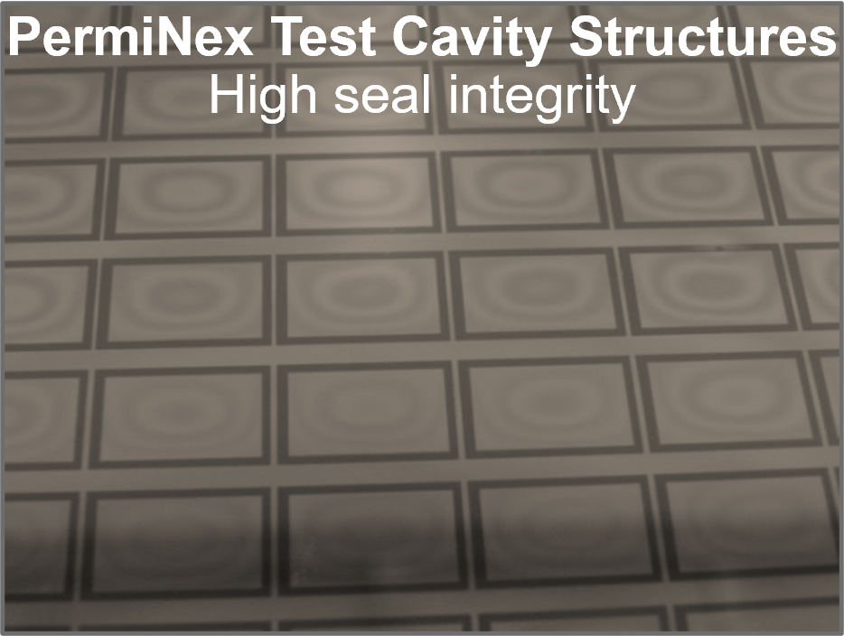
Test cavity structure bonded using PermiNex maintains vacuum seal due to strong bond. Image Credit: Kayaku Advanced Materials
Where do materials such as photo-patternable epoxies or wafer bonding adhesives fit into today’s device fabrication workflows?
A: Bonding typically occurs on the back end of a fabrication workflow and is particularly useful for packaging and device protection needs. Kayaku’s PermiNex® (1000 & 2000) series was formulated to provide low-temperature processing and thermal/mechanical robustness to accommodate myriad pre- and post-processing workflows.
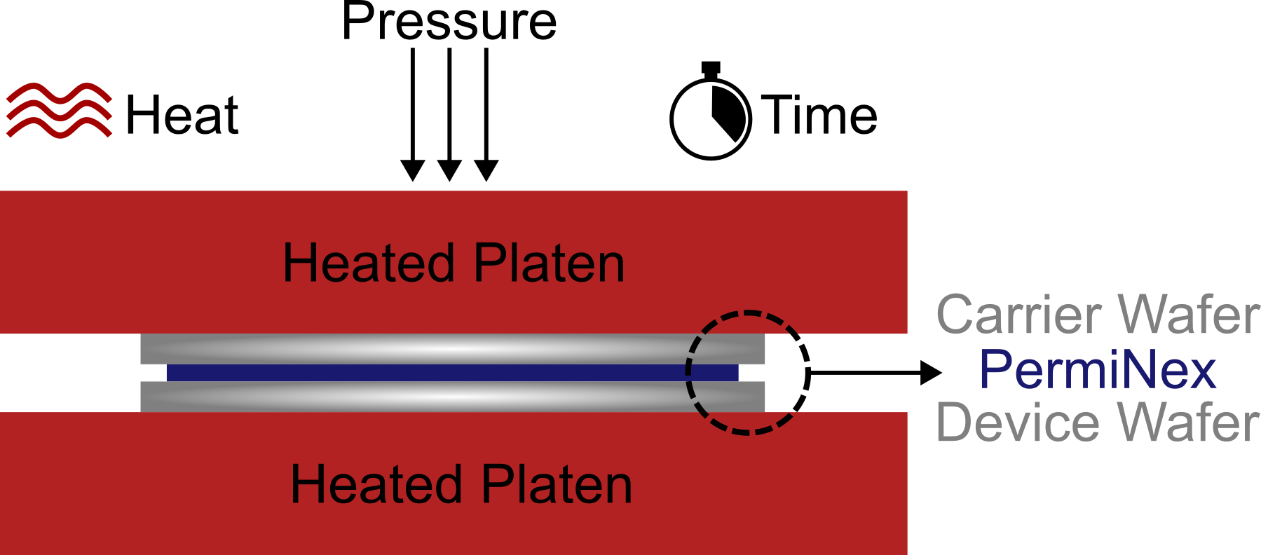
Schematic of typical wafer bonding process using PermiNex. Image Credit: Kayaku Advanced Materials
What are the main performance characteristics engineers should evaluate when selecting a photo-patternable bonding material, such as adhesion, resolution, bond strength, chemical resistance, thermal stability, or stress?
A: All are important, but not necessarily all at once. The main performance metrics will depend on the user’s specific device or planned usage of the bonded pair. For example, if the bonded pair is expected to withstand high-temperature bakes, the thermal stability is critical. But the material’s thermal stability can depend on temperature, time, and the baking environment (air, N2, etc.), so it is important to evaluate the material's functionality in its intended environment.
Fortunately, PermiNex® was formulated to provide a good balance of all important metrics: bond strength, resolution, adhesion to various substrates, chemical and thermal stability, and quick processing. Our team can help you optimize your processing to accommodate the metrics that are most important to your workflow.
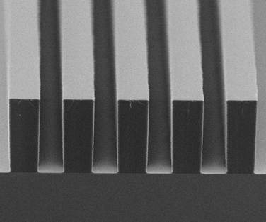
20 μm features in 40 μm thick PermiNex® 1000. Image Credit: Kayaku Advanced Materials
Photo-patternable materials often have to balance lithographic performance with long-term mechanical and chemical durability. How do you think about that trade-off during material design or process development?
A: When designing a new material or process, we focus on the end user and the most relevant application spaces. Some applications require high resolution, while others do not. Since it is unlikely to meet all the desired material properties, we focus on the most critical ones. Luckily, some can be tuned through process optimization, so we utilize that toggle whenever necessary.
What are some of the most common processing challenges customers face when implementing photo-patternable bonding, and how can those challenges be addressed early in development?
A: Challenges can span from overcoming topography to uniformity to unique device geometries and substrates. We recommend evaluating patterning success on the device substrate first, followed by evaluation of bonding success to the carrier substrate. Ensuring good patterning, adhesion, and planarity on the device substrate sets the customer up for success during bonding. Once the customer reaches the bonding step, several toggles, such as pressure and time, can improve the bond, and our team is available to help you optimize your process for your specific application.
How does photo-patternable bonding support the trend toward smaller, more complex, and more highly integrated devices?
M: As the industry pushes toward finer pitches, higher interconnect densities, larger package complexity, and heterogeneous integration, manufacturers are looking for ways to increase functionality without adding process complexity. Photo-patternable bonding enables precise definition of bond areas while eliminating additional processing steps associated with conventional bonding approaches. This becomes particularly important for advanced packaging, 3D integration, and emerging glass-based architectures, where space is limited and every process step impacts yield and scalability.
Kayaku Advanced Materials emphasizes close collaboration and engineer-to-engineer support. How important is process partnership when customers are moving from concept or lab-scale validation toward production?
M: Moving from proof-of-concept to production is often where the real engineering work begins. As customers scale, challenges around yield, reliability, and process integration become increasingly important. Through close engineer-to-engineer collaboration, combined with our in-house cleanroom and process expertise, we are able to help customers troubleshoot issues, optimize processes, and accelerate the path to manufacturing.
Looking into the future, where do you see photo-patternable bonding technology having the greatest impact, and what developments are you most excited to see in the years ahead?
A: I am excited to see photo-patternable bonding being implemented in more innovative, advanced packaging solutions across a variety of device types to enable high-performance 3D integration. The application space continues to grow, and we see photo-patternable bonding as an enabling material for microfluidics, co-packaged optics, MEMs, ICs, and more.
M: I am excited to see photo-patternable bonding support the broader trend toward heterogeneous integration. As devices become more integrated and three-dimensional, engineers are increasingly combining silicon, glass, polymers, and other materials within a single architecture while managing thermal budget and manufacturing complexity. Looking ahead, I see significant opportunities in hybrid bonding, smart sensors, flexible electronics, and photonic devices, where higher levels of integration are driving new device designs.
About Meg Nagesha

Meg Nagesha holds an MS in Microelectronic Engineering from Rochester Institute of Technology and a BE in Electrical, Electronics and Communications Engineering from CMR Institute of Technology. At Kayaku Advanced Materials, she supports semiconductor materials, advanced packaging, MEMS, and microfluidics through technical business development and customer-led innovation.
About Abigail Rendos

Abigail Rendos completed her PhD in Material Science & Engineering at Boston University. At Kayaku Advanced Materials, she has progressed from Engineer to Applications Engineering Manager, where she leads the Applications team and supports materials-focused engineering and development.

This information has been sourced, reviewed and adapted from materials provided by Kayaku Advanced Materials.
For more information on this source, please visit Kayaku Advanced Materials.
Disclaimer: The views expressed here are those of the interviewee and do not necessarily represent the views of AZoM.com Limited (T/A) AZoNetwork, the owner and operator of this website. This disclaimer forms part of the Terms and Conditions of use of this website.