PermiNex® 1000 and 2000 are epoxy-based, photo-patternable bonding materials designed for advanced wafer-level packaging, MEMS fabrication, and microfluidic device manufacturing. These materials enable precise adhesive layer definition and wafer bonding through high-resolution photolithographic patterning, eliminating the need for additional bonding films or complex assembly processes.
Overview
PermiNex® materials combine high-resolution photo-patterning with robust wafer bonding performance, making them ideal for cavity formation, wafer capping, and permanent bonding applications. Their unique photo-patternable bonding capability allows manufacturers to create precisely defined bonding structures while maintaining excellent alignment accuracy and bond integrity.
Processed at temperatures below 200°C, PermiNex® materials deliver strong adhesion, fine feature resolution, and reliable bonding performance across a variety of substrates, including silicon and glass. This combination of design flexibility and process compatibility makes PermiNex® an ideal solution for advanced semiconductor, MEMS, and microfluidic applications.
A typical bonding process for PermiNex series is included below with relevant processing variables such as time, temperature, and pressure.
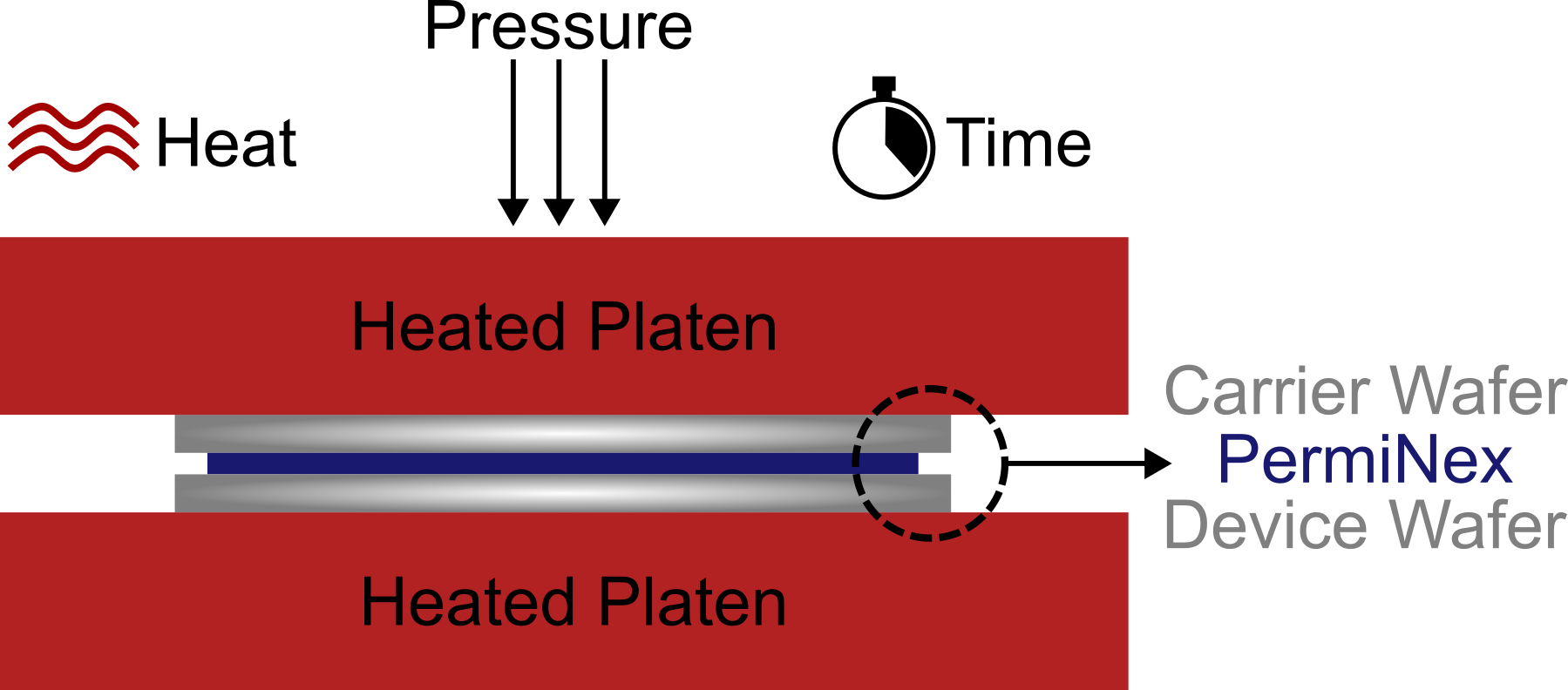
Image Credit: Kayaku Advanced Materials
Key Features
- Photo-patternable bonding materials for wafer-level manufacturing
- Negative-tone, photo-imageable epoxy chemistry
- Available in solvent-developable and alkaline-developable formulations
- High-resolution patterning for precise bond-line definition
- Low-temperature processing (<200°C)
- Strong, void-free wafer bonding performance
- Excellent adhesion to silicon, glass, and other common substrates
- High reliability performance (HAST, TCT)
- Compatible with downstream processes including dicing, soldering, and assembly
Material Uses
- Wafer bonding
- Cavity formation and wafer capping
- MEMS packaging
- Microfluidic device fabrication
- Backside processing support
- Thin-wafer handling and support
- Through-silicon via (TSV) processing
- Temporary and permanent wafer bonding workflows
Industry Applications
- Microfluidics
- 3D integration and TSV manufacturing
- Advanced semiconductor packaging
- Compound semiconductor manufacturing
- MEMS fabrication
- Power device processing (Si, SiC, GaN)
- Thin-wafer and fragile substrate processing