In this interview, industry expert Dr. Andrew Strudwick explores how printed electronics and 2D materials are enabling new sensing applications, flexible devices, scalable manufacturing, and emerging opportunities across healthcare, industry, and beyond.
For those who may not be familiar with it, what is the Graphene Engineering Innovation Centre, and how does it work with organizations looking to develop new technologies?
The Graphene Engineering Innovation Centre, or GEIC, is an industry-led innovation center at The University of Manchester, based in the Masdar Building on Sackville Street. It opened in December 2018 as a £60 million facility, and it sits alongside the National Graphene Institute as the applications and scale-up end of Manchester's graphene ecosystem.
While the NGI focuses on fundamental research, the GEIC exists to close the gap between what works in a research paper and what works on a production line.
Practically, that means pilot-scale equipment and specialist teams across eight capability areas: printed electronics, coatings, composites, construction materials, energy storage, membranes, deposition and integration, and measurement and characterization.
A company can come to us with a material, a formulation or an application idea and work through synthesis, formulation, prototyping, characterization and pre-production validation in one place.
How companies engage varies. Some join as tiered partners with ongoing access to the facilities and teams; others come to us for a defined, shorter piece of project work to answer a specific question or de-risk a specific step. We work with everyone from micro start-ups and SMEs through to multinationals, and at every stage from early exploration to commercial deployment.
In every case it starts with a conversation about what the company is actually trying to achieve, and we shape the work from there.
What kinds of challenges are companies typically bringing to your printed electronics team, and where do you tend to get involved in the development process?
If I start at the end of that question, we often get involved in printed electronics at an early stage, when a company has an idea about how a printed circuit might help in their application area. We then help with initial design and prototyping, often using screen printing, but we also have other techniques such as inkjet and direct-write printing, which can be effective at the prototyping stage. We will do some initial testing and then help them carry that through into the next iterations.
In terms of what kinds of problems we look at, that is certainly varied. We have applications from embedded heating systems, for de-icing in automotive or aerospace applications, for example. We also look at printed biosensors, similar to what people might be familiar with in blood glucose sensing, and we have worked on smart materials: things like strain or impact sensors embedded within a system or device.
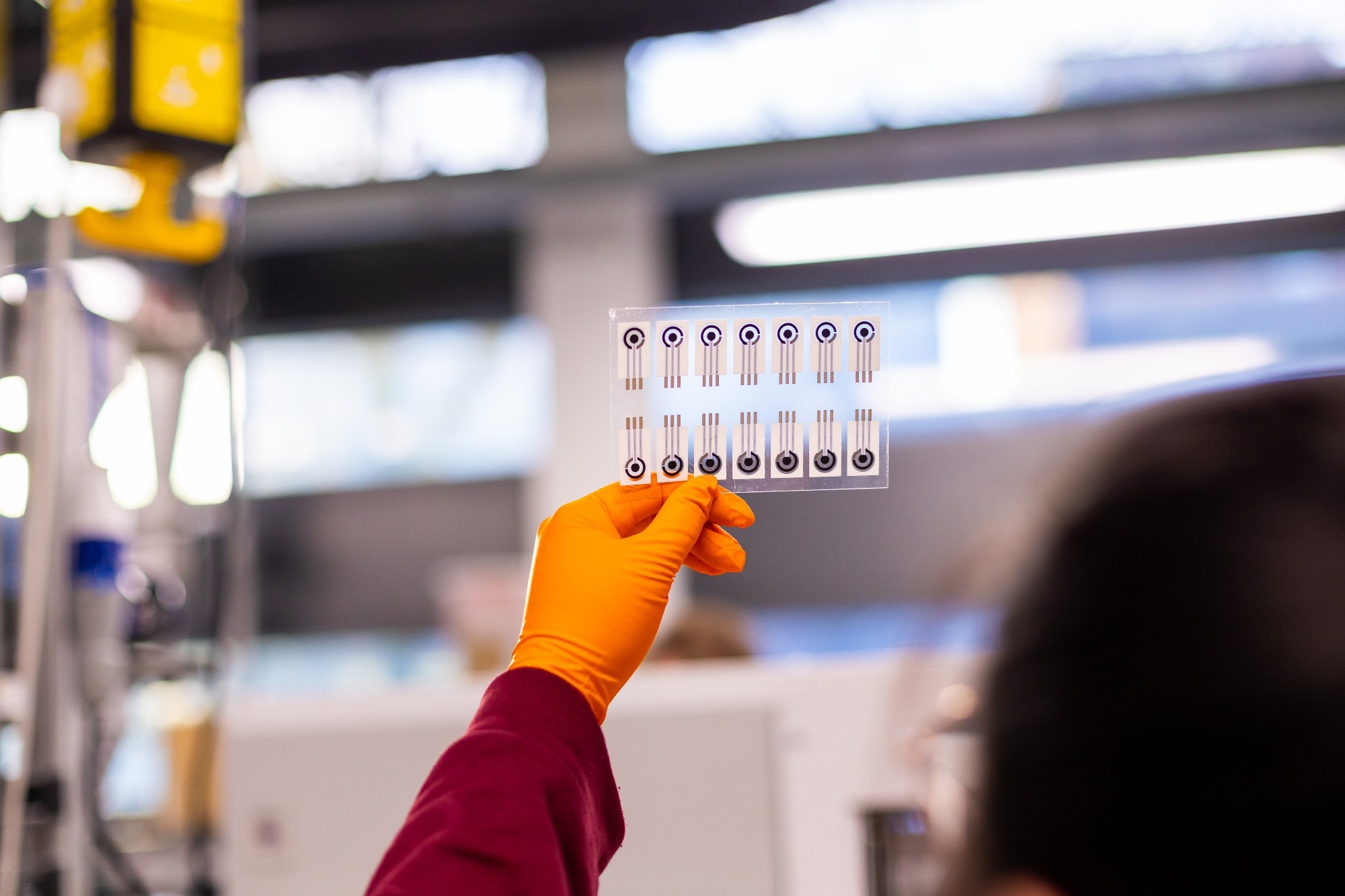
Image Credit: Graphene - The University of Manchester
What makes graphene and other 2D materials particularly interesting for printed electronics compared with more conventional electronic materials?
One key driver at the moment is the cost of silver. Silver has been a very standard material in this sector and its price has been rising quickly, so alternatives are being sought. Graphene inks, and graphene and silver hybrids, are of real interest in this context.
There are other benefits to graphene beyond cost. Because it is carbon-based, you can graft functional groups onto its surface, making it very useful for biosensing and gas sensing. It has relative chemical inertness, so you avoid the oxidation effects you get with silver inks. And graphene ink, once printed, tends to be more flexible than silver and other metallic inks, so you can use it in genuinely flexible applications.
Among the other 2D materials, boron nitride is attracting a lot of interest at the moment as an insulating material. It has the interesting combination of being thermally conducting but electrically insulating, and as we push chip performance, materials that can take heat away while maintaining electrical insulation are of real interest.
Which applications for 2D material-enabled printed electronics are showing the greatest potential at the moment, and what is driving interest in those areas?
I think the biggest driver is increased levels of data acquisition in what would previously have been fairly ordinary, everyday systems. The overarching term for that is the Internet of Things: the ability to generate data where we previously could not, by embedding electronics within systems.
There is also a driver in enabling new material solutions to problems; hydrogen storage is a good example. If you want to move away from metallic containers to more lightweight carbon fiber containers, there are concerns about delamination in those systems.
The ability to embed a strain sensor in a carbon fiber composite storage system, generating continuous data so you can offset that risk and observe whether delamination is occurring, could make that material type viable for that application.
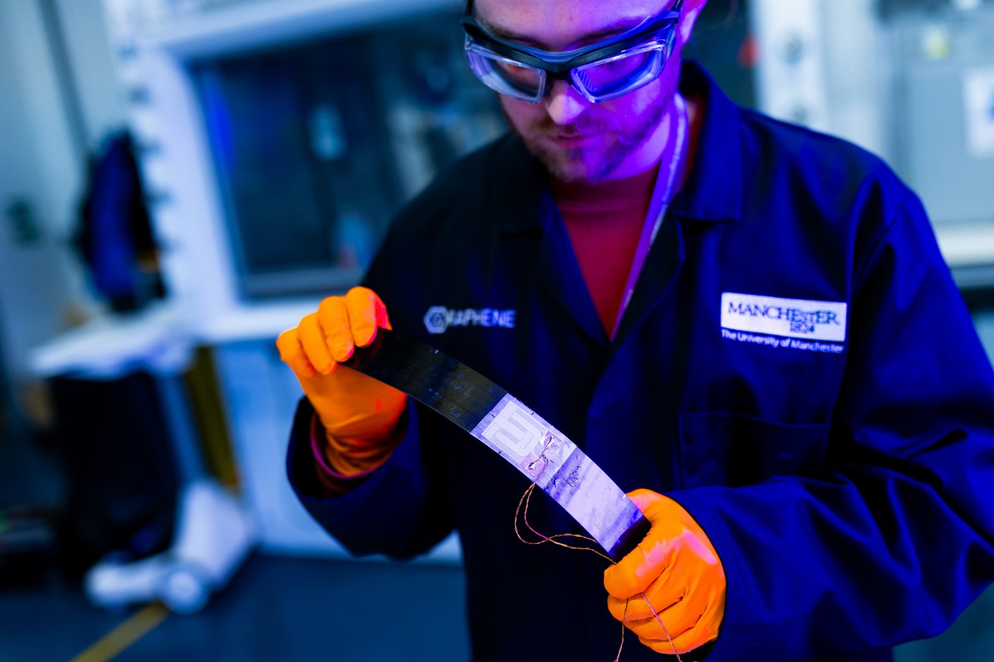
Image Credit: Graphene - The University of Manchester
Which industries do you think stand to gain the most from advances in printed and flexible electronics over the next few years?
Our scope is quite broad, so my honest answer is that it could be almost anyone. Anyone with a system who would like increased functionality on a surface or within a panel could benefit.
Healthcare is probably one of the earlier adopters. Again, it comes back to the Internet of Things, allowing data to be generated when people are away from a hospital setting, in their own homes.
This helps with an aging population and with monitoring people remotely: keeping track of vital signs or knowing whether someone has had a trip or a fall. So, healthcare is a key area set to advance. But as I say, it is really anywhere you might want data that is currently not available to you.
Developing a functional material in the laboratory is very different from manufacturing it at scale. What are some of the biggest hurdles involved in moving printed electronics from an early prototype towards commercial production?
Having a supply chain in place to do this really helps, and the good news is that large-scale printed electronics processes do already exist. Many LCD screens contain printed electronic components, and commercial electronic systems increasingly use printing methods in their manufacture. There are companies out there who can offer printing at scale.
We are more often involved in materials derisking, incorporating advanced materials into the inks to provide that increased functionality. Alongside that, we have conversations with the supply chain to make sure the processes we are using at lab scale are applicable at the next scale up, and potentially at the scale after that. That is the piece that stops a promising prototype from stalling later on.
Sensors are one promising area for printed electronics. Where do you see the most exciting opportunities for printed sensing technologies in areas such as healthcare, infrastructure, or environmental monitoring?
Healthcare is where a lot of the immediate opportunity sits. Printed biosensors are a well-established route, with blood glucose sensing as a familiar example; beyond that, there is remote patient monitoring: printed, flexible devices that can sit on or near a person at home and track vital signs or detect a trip or a fall.
With an aging population and pressure on hospital settings, being able to generate that data outside the hospital is very valuable.
On the infrastructure and structures side, the interesting work is in strain and impact sensing embedded within a material rather than bolted onto it.
The example of hydrogen storage is a good one. A strain sensor printed into a carbon fiber composite vessel, giving you continuous data on whether delamination is beginning, changes the risk profile of using that material at all. The same logic applies anywhere you have a structure whose condition you currently have to inspect rather than monitor.
For gas and environmental sensing, graphene's chemistry is the enabler. Because it is carbon-based, you can graft functional groups onto the surface to make it selective for particular species, and its relative chemical inertness means it holds up well in service. The common thread across all three areas is the same: printed sensing lets you put data generation where it has not been possible before.
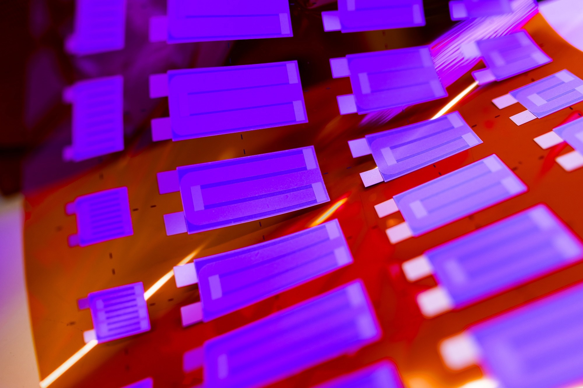

Image Credit: Graphene - The University of Manchester
What opportunities do printed electronics create for developing devices on unconventional surfaces or substrates that would be difficult to address using traditional electronics manufacturing?
I personally come from a background of growing graphene and 2D materials using processes such as chemical vapor deposition. One of the problems we ran into then, and still run into, is that a lot of the surfaces you would like to coat simply cannot handle the process temperatures that CVD, PVD, and similar coating methods require.
What printed electronics allows, by producing platelets of these materials in ink form, is the handling of polymeric and flexible substrates that are otherwise off-limits unless you use a transfer process. So there is a real benefit there.
There are also printing methods that enable printing onto non-flat surfaces, such as curves or structures with more complex geometry, often using robots on production lines. Spray coating and printing-adjacent techniques mean you can effectively spray devices onto surfaces where that is appropriate.
But processing conditions are the main point. There is no need for high temperatures or high-vacuum systems; you can do this under ambient lab conditions, and the substrate typically does not need to reach above around 150 °C during curing.
Sustainability is becoming increasingly important in electronics manufacturing. Where could printed electronics and 2D materials help reduce the environmental impact of future devices?
It is a good question, and it is something we have to be careful about, because when you embed electronics into a system that previously had none, you are adding another set of materials that must be considered in the recycling process.
That is again where graphene has an advantage over metallic inks. Being carbon-based, it is often easier to integrate into existing recycling streams.
Beyond the material choice itself, it comes down to making sensible decisions early. You need to be sure the materials are appropriate for the application area, with an end-of-life view in mind, so that when the sensor or device has done its job, you have already thought about how it gets recycled.

Image Credit: Graphene - The University of Manchester
When companies first approach the GEIC with an idea involving printed electronics, what are some of the most common misconceptions or technical challenges that need to be addressed?
We have not had too many misconceptions, to be fair. The one that does come up is that people will read the literature and see the electronic or thermal behavior of perfectly formed graphene or 2D materials, meaning material exfoliated at a very small scale into single flakes and tested at the micron level.
Those figures, and especially the electrical conductivity of graphene, are not directly transferable when you are using platelets of the material within an ink. You do get a performance, and often a very useful one, but it is not the headline number people might have read in a paper. So there are usually some conversations around managing expectations on that.
Other than that, those initial conversations are often the best part of the process, because we learn as much from our partners as we are able to tell them.
Looking further ahead, what developments in materials, manufacturing or device design do you think could have the biggest impact on the next generation of printed electronics?
On the material side, I think everyone is starting to get excited about MXenes. In printed ink, they really do appear to offer extremely promising electrical conductivity and other properties that will make them very interesting in this application area.
When considering processing, everyone is continually pushing the envelope depending on their application. People will keep pushing printed and screen designs in screen printing, particularly on resolution and print speed, and will vary materials quickly within those processes to generate hybrid stacks. I think all of those will continue to be pushed, and they will take the sector forward.
Your upcoming event on November 3rd focuses on bringing 2D materials closer to commercial applications. What do you hope attendees will come away understanding about the opportunities in this field?
When we get people through the door here at the GEIC, it almost always sparks ideas. It gives people a feel for the art of the possible, for what can actually be achieved. Very often it shows people what we do and then prompts ideas they were not walking in with.
There will be a tour on the day, and when we take people round, as I say, it opens both eyes and ideas. Hopefully it also sparks conversations about potential collaborations. There will be other industry partners and external representatives in the room, so these conversations might take place during the networking sessions instead. That is great too; it pushes things forward across the whole ecosystem.
So really, I hope it stimulates ideas and conversations about how to collaborate and move forward as a sector as a whole.
Join the event! 3rd of November at the GEIC
Who would benefit most from attending this event, and why is now a particularly useful time for organizations to explore what printed electronics could offer them?
At the GEIC in general, we work with all types of companies, from micro-sized start-ups and SMEs right through to multinationals; all are welcome. I think we add value to all of the companies we work with, in slightly different ways, but the value is there.
On the graphene and 2D materials side, there is good momentum, with a number of commercial products now coming through to market, which is starting to de-risk their use in real products and final applications. Ten years ago it might have felt high-risk to look at a 2D material solution; there is now enough out there in the market to suggest that is no longer the case.
At the same time, it is still early enough that companies might gain a market advantage over competitors by looking now. There is probably still that first-to-market jump available.
About Dr. Andrew Strudwick 
Andrew Strudwick holds a Master’s degree in Physics and a PhD from the University of Leeds, where his doctoral research focused on epitaxial graphene for nanoelectronics. At the University of Manchester, he has progressed from Application Specialist to Application Manager at the GEIC, leading industrialisation projects involving graphene and 2D materials.

This information has been sourced, reviewed and adapted from materials provided by Graphene Engineering Innovation Centre (GEIC).
For more information on this source, please visit Graphene Engineering Innovation Centre (GEIC).
Disclaimer: The views expressed here are those of the interviewee and do not necessarily represent the views of AZoM.com Limited (T/A) AZoNetwork, the owner and operator of this website. This disclaimer forms part of the Terms and Conditions of use of this website.