From nanoscale materials engineering to advanced inspection and process control, this collection shows that precision and reliability underpin performance across modern device architectures.
Download the eBook
This Semiconductor Analysis and Manufacturing Industry Focus eBook, sponsored by Avantes, explores the technologies, materials, and analytical strategies driving next-generation semiconductor innovation.
Advances in functional materials are showcased through developments in polydopamine nanosheets for enhanced artificial photosynthesis, atomic-level improvements in indium phosphide nanoclusters for superior light emission, and the growing role of spectroscopy in optimizing perovskite photovoltaics. These innovations reflect the increasing importance of material design in enabling energy-efficient and high-performance semiconductor applications.
Material quality and fabrication processes remain central themes. Ultra-pure materials are highlighted as essential for minimizing defects, while spectroscopy-driven approaches to thin film fabrication demonstrate how controlled deposition and characterization support device integrity. Complementing this, detailed insights into silicon wafer manufacturing and the use of optical emission spectroscopy for plasma monitoring underline the importance of process precision and real-time diagnostics.
Finally, the eBook addresses inspection and reliability, from next-generation imaging techniques enabling advanced defect detection to the impact of environmental test conditions on failure analysis. Together, these insights provide a comprehensive overview of the tools and innovations shaping semiconductor analysis and manufacturing.
Download the eBook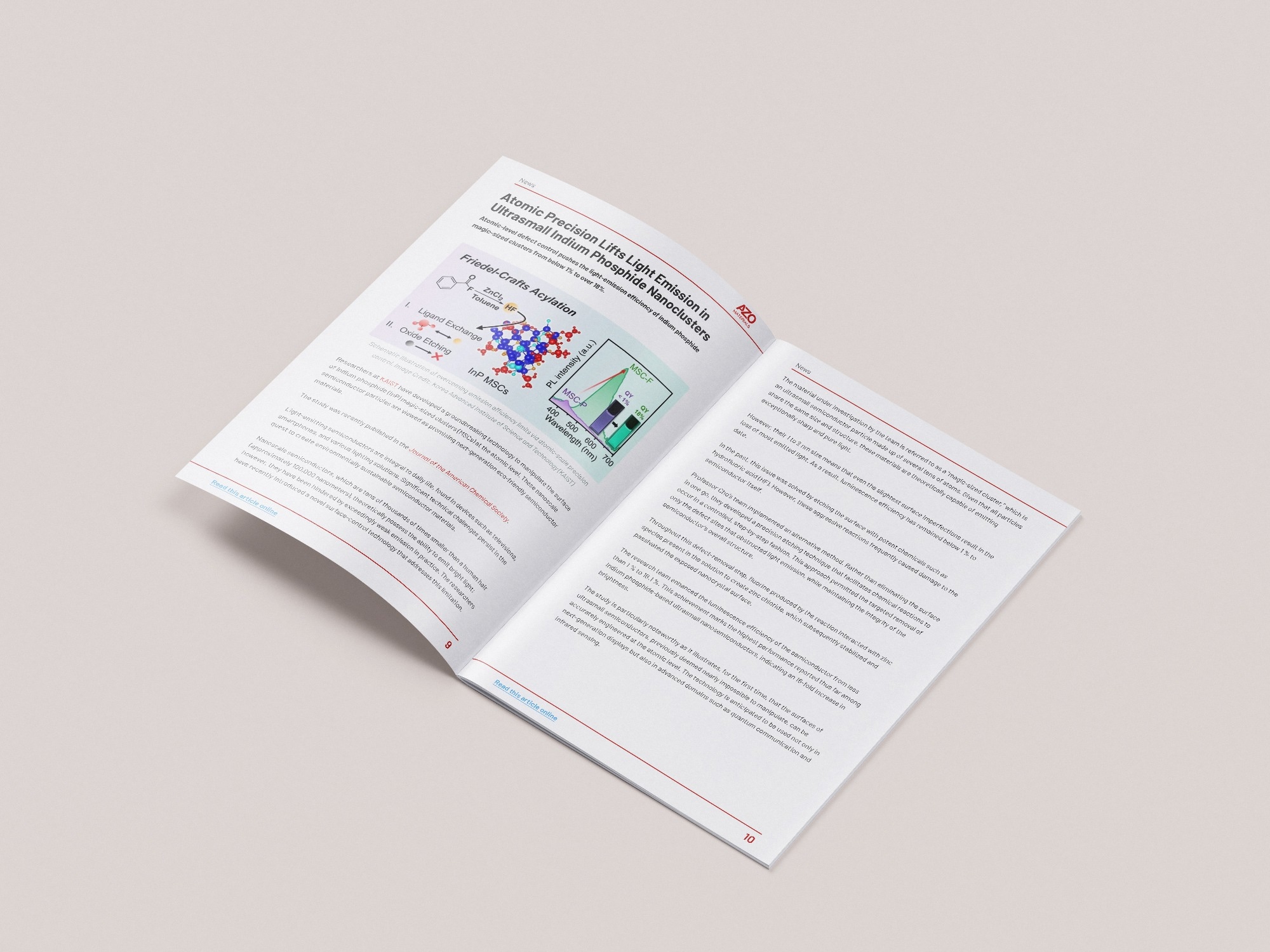

This information has been sourced, reviewed, and adapted from materials provided by Avantes.
For more information on this source, please visit Avantes.