Sponsored by AvantesReviewed by Maria OsipovaApr 23 2026
Thin films are widely used across a range of sectors, including microelectronics, display technologies, semiconductors, and optical elements. This technology has enabled many of the technological breakthroughs currently in use.
The need for precise control over the thickness of each layer during the epitaxial growth process is a constant consideration, regardless of the material’s end use.
This can be especially challenging with these films, given their extreme thinness, typically ranging from 1 nm to 100 microns. Three common techniques are currently used to quantify surface thicknesses at this scale: stylist profilometry, ellipsometry, and spectral reflectance.
Stylist profilometry technologies, such as atomic force microscopy, can achieve sub-nanometer resolution, but their contact nature can cause surface damage and require extremely long measurement times.
Spectral reflectance and ellipsometry, conversely, are both non-contact optical techniques able to scan large areas with little to no sample preparation.
Ellipsometry is relatively useful, but this technology is generally larger and more expensive than spectral reflection because it requires multiple polarizations and off-axis measurement angles. In contrast, spectral reflectance is a polarization-independent technique performed at normal incidence, significantly reducing the system’s cost and complexity.
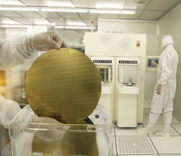
Hands holding a silicon wafer in a clean room laboratory, semiconductor production. Image Credit: Avantes
Effects of Film Thickness on Spectral Reflection
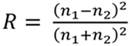
A certain percentage of light is reflected back from the interface whenever light propagates from one material to another. The equations governing this interaction can be cumbersome, but at normal incidence they reduce to a simplified expression that depends solely on the difference between the two indices of refraction.
Equation 1 shows how the reflectance (R) of non-absorbing materials is equal to the square of the difference in index (n1 and n2), divided by the square of the sum of the two indices.
This simple equation governs many everyday physical phenomena, for example, the way a person can see themselves in a transparent window when it is dark. Many modern-day optoelectronics also leverage this relationship to improve performance and reduce cost, including LEDs and laser diodes.
 |
Equation 1 |
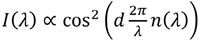
When dealing with spectral reflectance from a single-layer thin film, there are two interfaces that cause reflections: the air-film interface and the film-substrate interface.
Depending on the film’s thickness and the index of refraction, this will cause light reflected from each surface at a particular wavelength to have a slight phase difference, resulting in destructive or constructive interference.
A material’s index of refraction is wavelength dependent, meaning this phase difference will vary across the spectrum of a broadband light source. Equation 2 shows how this wavelength-dependent interference pattern results in a chirped sinusoidal spectrum; the thicker the film, the higher the chirp frequency.
In this equation, d represents the film’s thickness, n(λ) represents the index of refraction as a function of wavelength, λ represents the wavelength, and I(λ) represents the intensity as a function of wavelength.
 |
Equation 2 |
Equation 2 makes several assumptions and simplifications, but it is useful for visualizing how spectra vary with film thickness.
Figure 1 presents an idealized example of this type of spectrum for MgF2, clearly showing a chirped spectrum whose frequency increases with increasing film thickness.
The majority of dielectric materials absorb at least some light as it propagates through the material. This property can be described mathematically through the material’s complex index of refraction, n*(λ) = n(λ)+ik(λ), where n is the index of refraction, and k is the absorption coefficient.
While the absorption coefficient is ‘imaginary’ from a mathematical perspective, it is a very real property that must be taken into account to accurately model the ‘real’ reflectance spectrum for a specific film thickness.
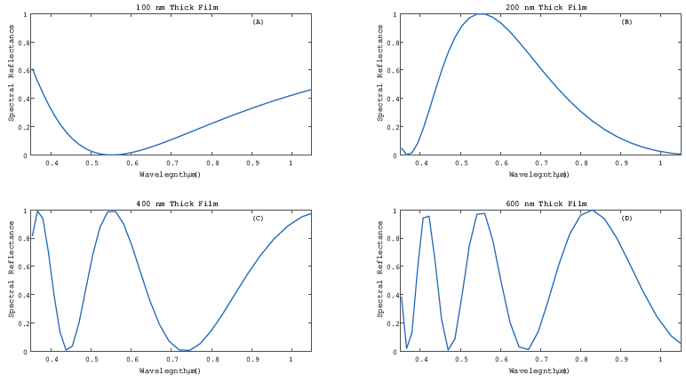
Figure 1. Theoretical reflectance spectra (assuming no absorption) for a MgF2 thin film with (A) 100 nm thickness, (B) 200 nm thickness, (C) 400 nm thickness, and (D) 600 nm thickness. Image Credit: Avantes
Typical Spectral Reflection Setup
The setup of a thin film spectral reflection measurement system is much like that of a traditional reflectance system, but the probe angle differs. The illumination and collection sources must be normal to the surface of the sample in this instance, as opposed to the 45 ° angle employed in the majority of reflectance measurements.
This setup includes: a fiber-coupled spectrometer like Avantes’ AvaSpec-VARIUS™, a deuterium halogen light source, such as the Avalight-DH-S-BAL, and a fiber optic reflection probe such as the Avantes FCR-7UV200-2-ME. Stable fixation of the probe tip should be ensured, as well as an equal stand-off distance between the probe and reference and between the probe and samples.
Figure 2 shows an example of a typical setup.
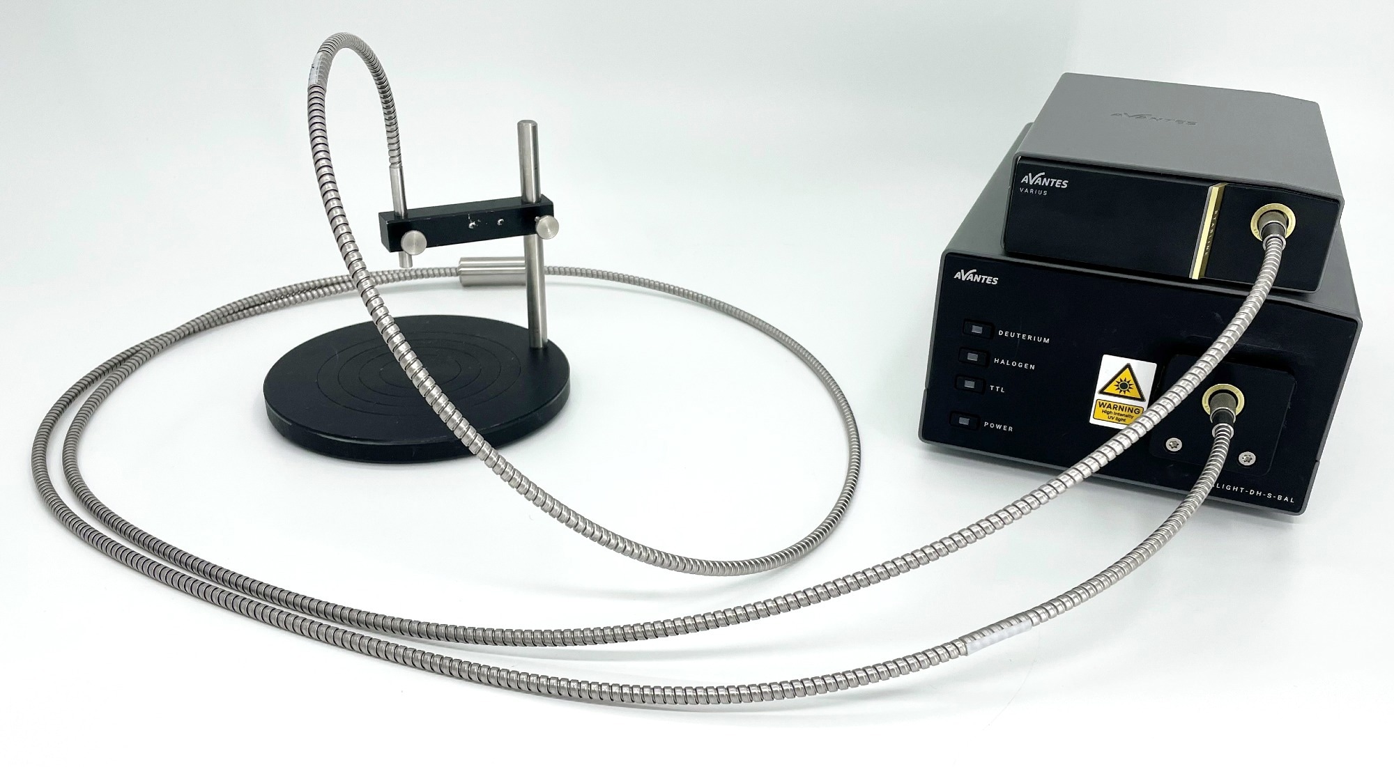
Figure 2. Typical experimental set-up for thin film thickness measurement by spectral reflection. Image Credit: Avantes
Performing a Measurement
The measurement process starts with the user acquiring a reference spectrum from an uncoated reference substrate to normalize the spectrometer and calculate an accurate reflection spectrum.
The reference substrate is then replaced with the coated substrate, which is measured under the same conditions. The AvaSoft software (Figure 3) can determine the film thickness once the reflectance spectrum has been measured.
It is important that both the substrate thickness and material, and the thin film design thickness and material are inputted into the software to enable the most accurate measurement. Using this data, the software searches its database of material indices of refraction and absorption coefficients to correlate the measured reflectance spectrum with a theoretical curve of a specified thickness.
Figure 3 shows an example of a reflectance spectrum for a 655 nm SiO2 thin film coated on a Si substrate. This was generated using the AvaSoft software platform’s thin film measurement module.
A built-in library of common substrate and film materials is available, but the user can also create their own ‘*.nk’ file by entering an array of indices (n) of refraction and coefficients of absorption (k) for each specific wavelength of interest.
Summary
Engineers can now rapidly and cost-effectively test film thickness at all stages of the manufacturing process by employing spectral reflectance in the thin film measurement process.
Avantes offers a comprehensive portfolio of fiber-coupled miniature spectrometers, probes, and light sources, which, when combined with the company’s AvaSoft Thin Film software module, support the measurement of single-layer thin films ranging from 10 nm to 50 μm in thickness with a resolution of one nm.
Multilayer software options are available through Avantes, as well as a range of optional thin-film standards. These standards provide sample uncoated and coated substrates for validation purposes, allowing the reliability and repeatability of the process to be verified.
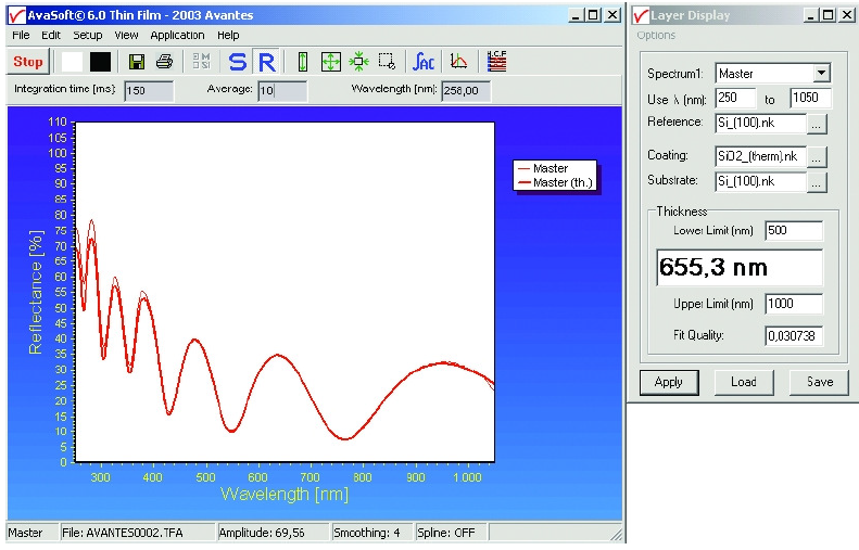
Figure 3. Screenshot of the spectral reflectance spectrum for a SiO2-coated Si substrate, showing a calculated film thickness of 655.3 nm.
Avantes’ Avaspec instruments are well-suited to continuous and high-speed triggered measurements, like those required in the fabrication of thin films.
Each spectrometer presented here is also available as an OEM module, allowing integration into multichannel rack-mount systems, which are ideally suited for thin-film process monitoring.
These instruments can communicate via Ethernet, USB, and the native digital and analog input/output capabilities provided by the Avantes AS7010 electronics board, enabling a superior interface with other devices.
The Avantes AvaSpec DLL software development package also includes sample programs in Visual Basic, C#, C++, Delphi, LabVIEW, MATLAB, and other programming environments, enabling users to develop their own code for thin-film applications.
This software development kit is especially useful when integrating instruments into an automated sampling system or when analyzing complex multi-layer thin films with customized code.

This information has been sourced, reviewed, and adapted from materials provided by Avantes.
For more information on this source, please visit Avantes.