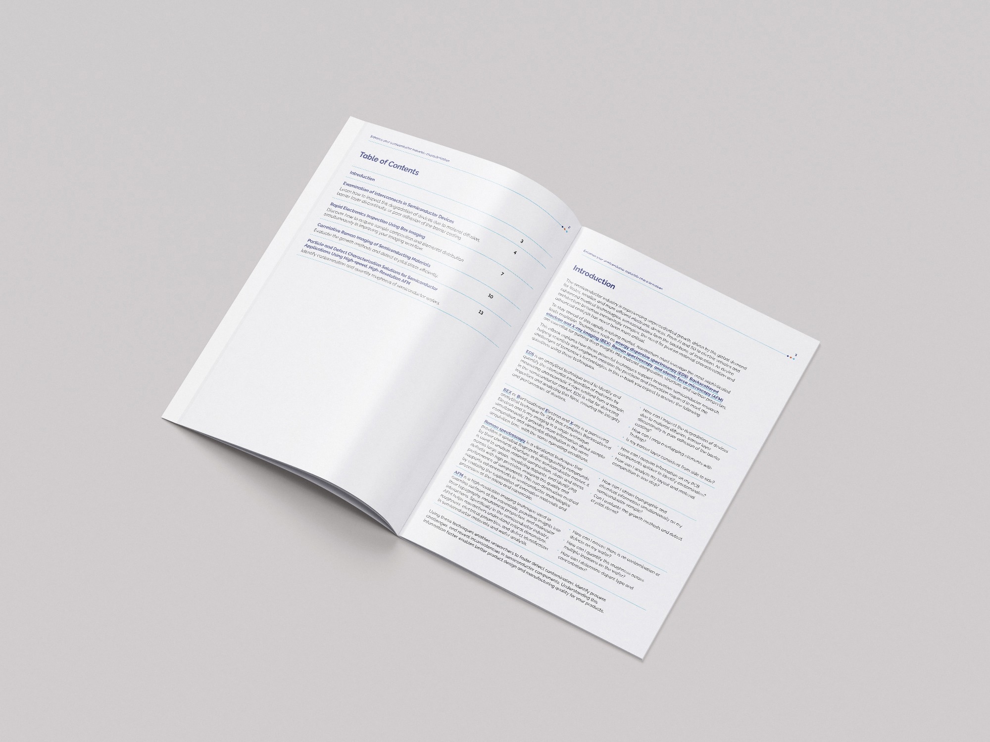
The semiconductor sector is witnessing extraordinary growth, driven by global demand for quicker, smaller, and more efficient electronic products. From artificial intelligence and 5G to electric vehicles and improved medical treatments, semiconductors are the foundation of innovation.

As device architecture becomes more complicated, precise material characterization and advanced analysis become even more important. Researchers must use the most advanced technologies available to keep ahead of this fast-changing market.
Energy dispersive spectroscopy (EDS), backscattered electron and X-ray imaging (BEX), Raman spectroscopy, and atomic force microscopy (AFM) are critical techniques for acquiring a thorough understanding of material composition, structure, and surface properties.
This eBook explores how these powerful technologies promote new semiconductor research, assisting scientists and engineers in maintaining the precision and ingenuity required to tackle tomorrow's technological challenges. This e-book will use these strategies to answer the following questions.
Questions:
- How can I inspect device degradation caused by material diffusion, discontinuities in the barrier layer, or poor coating adhesion?
- How can I quickly gather information on PCB components to identify contaminants?
- How can I simultaneously collect topographic and chemical information on a semiconductor sample?
- How can I prevent contamination or faults on my wafers?


 Download the full eBook now to learn more

This information has been sourced, reviewed and adapted from materials provided by Oxford Instruments America.
For more information on this source, please visit Oxford Instruments America.