In confocal Raman imaging, the acquisition time for one Raman spectrum is a vital value, because it affects the acquisition time of the image which usually contains tens of thousands of Raman spectra. This article shows how a spectroscopic EMCCD is used as a detector to considerably reduce the acquisition time down to a few milliseconds per spectrum and also to dramatically improve the overall sensitivity.
Working Principle behind Confocal Microscopy
A point light source (laser) is used by confocal microscopy which is focused onto the sample. The reflected (fluorescence) light is often collected with the same objective and then focused into a pinhole in front of the detector. This makes sure that only light from the image focal plane reaches the detector, which robustly increases the image contrast and, with appropriate selection of pinhole size, somewhsat increases the resolution.
In confocal Raman imaging, as in the alpha300 R system which was employed for the experiments described here, exclusive filters are used to suppress the reflected laser light while allowing the Raman scattered light to be detected with a combination of spectrometer and CCD camera. In order to achieve an image, thousands of spectra are obtained in a very short time with typically less than 100 ms integration time for each spectrum.
Since the Raman scattering cross section is extremely small and the excitation power is restricted to a few milliwatts, how can one improve the overall sensitivity of a confocal Raman system?
Optimizing S/N Ratio Improves Overall Sensitivity of CRM System
It is important to optimize signal-to-noise ratio (S/N). The initial step is to enhance the collected Raman signal, and this can be achieved by optimizing the throughput of the spectrometer and microscope and by employing an objective with a high numerical aperture (NA). With the confocal setup, unwanted background signal from out-of-focus areas is reduced and S/N is further improved.
The Use of an Appropriate Detector with the Highest Sensitivity
Next is the option of a suitable detector with the highest sensitivity, for example a back-illuminated CCD, which can have more than 90% quantum efficiency. The readout noise and the dark noise are the main sources of noise of the detector itself. The objective should be to eliminate all other noise sources, so that the photon shot noise is the only one that remains.
Since photons follow the Poisson statistic, for a given signal the uncertainty is the square root of the signal in electrons. In the absence of other sources of noise, S/N cannot be greater than 10 for a signal of 100 electrons.
Dark Noise Reduces the Cooling Efficiency of the CCD
Dark noise is attributed to thermally generated carriers in the CCD, which can be considerably reduced through efficient cooling of the CCD. A good CCD has a thermal dark current of less than 0.01 electrons/pixel/second at -60 °C. Hence, it is not necessary to cool below -60 °C for integration times of a few seconds. As in the confocal Raman setup, dark current is completely negligible for less than 100 ms integration times. Readout noise is generated while changing the collected electrons into digital counts and is restricted by both the quality of the CCD's readout amplifier and the speed (digitization rate) of the readout process. The camera manufacturer specifies the readout noise, which is given in electrons. Typical values are 5-10 electrons for a 50 kHz readout rate to approximately 30 electrons for a 2.5 MHz readout rate.
The Readout Noise Limit
The signal is said to be readout noise limited if the readout noise exceeds the photon shot noise. In usual spectroscopic experiments, the integration time would be simply increased to obtain sufficient signals to make sure that the signal is shot noise limited again. However, this is not always possible in confocal Raman microscopy.
If an image consisting of 128 pixels/line and 128 lines is acquired with an integration time/spectrum of just 1 seconds, the total acquisition time would be 4,5 hours, which is reduced to less than 30 minutes for an integration time of 100 ms or to less than 3 minutes for an integration time of 10 ms. However, the faster the read out of the detector is, the noisier the readout amplifier gets.
A 1024x128 pixel CCD fitted with a 50 kHz readout amplifier can be read out in approximately 22 ms, which also happens to be the shortest possible integration time. Assuming a readout noise of 10 electrons, every signal below 100 electrons/pixel will be readout limited (Poisson noise < readout noise). For a fast readout amplifier, if the readout noise is 30 electrons then even a signal of 900 electrons (~ 1000 photons/pixel on the detector) will be readout limited.
What is an Electron Multiplying CCD
An electron multiplying CCD (EMCCD) is a standard CCD with an extra readout register which is driven with a much higher clock voltage than a usual CCD readout register. Owing to this high clock voltage, an electron multiplication through impact ionization is obtained with an adjustable total amplification of the signal of up to 1000 times. With this setup, the signal can always be amplified above the readout noise so that the S/N ratio is invariably restricted by the Poisson noise of the signal, even with the use of a fast readout amplifier. As an example, a 1600 x 200 pixel EMCCD with a 2.5 MHz readout amplifier, as used for the experiments in this article, can be read out in just 2.3 ms.
Calculations Showing the Improvements in S/N for Different Signals
The calculations given below demonstrate the enhancements in S/N that can be expected for different signals. It is assumed that CCD has 90% quantum efficiency (QE) and that signal amplification is set to a value at which a single A/D count equals the number of electrons of the readout noise (1 A/D count = 30 electrons for a 2.5 MHz readout amplifier).
If 100 photons fall on a CCD pixel in a specified integration time, 90 electrons will be generated and transformed to 3 A/D counts. The Poisson noise will be 9.5, which is about 0.3 A/D counts, and the readout noise will be 1 A/D count. With these numbers, the S/N ratio is approximately 2.6.
In an EMCCD, the electron gain factor will multiply the signal which can be as high as 1,000. Generally, a smaller amplification factor would be used, but it does not make a difference for the calculation, 90 electrons will be amplified to 90,000 electrons resulting in 3,000 A/D counts. The Poisson noise is 9,500 electrons which convert to 317 counts, whilst the 1 count readout noise is entirely negligible. S/N is 9.5, which is an improvement of a factor of 3.6.
If the signal is just 10 photons, this will result in a signal of just 0.3 counts for a standard CCD, but Poisson noise can be overlooked in this case. With 1 count readout noise, S/N is just 0.3 which is hardly a detectable signal. For an EMCCD, the signal is 333 counts and Poisson noise is 100 counts which provides a S/N of 3.3 – an improvement of 11 times over a normal CCD.
Actually, the electron multiplying process itself adds an extra, so called excess noise factor of approximately 1.4, so that the real improvements in S/N are reduced to 2.6 and 7.9, respectively for the examples described above.
In the case of higher signals, where the signal intensity is no longer readout limited, the excess noise factor of the EM process reduces the EMCCD’s S/N ratio to less than that of a normal CCD. Here, the EM register can be switched off and the "normal" readout register can be used. Therefore, the EMCCD works just as a usual back-illuminated CCD.
Confocal Raman Images of Polymer Samples
Shown in Figure 1 are three confocal Raman images of a very thin PMMA film, spin-coated onto a glass substrate. In the middle of the images, a vertical scratch was made with a metal needle in order to remove the PMMA layer. The film thickness, as determined with an AFM across this scratch, was 7.1 nm. Also, it was seen that there was an extra contamination layer of 4.2 nm thickness. At first, the material composition and origin of this contamination layer was not known but can be established by the confocal Raman measurement.
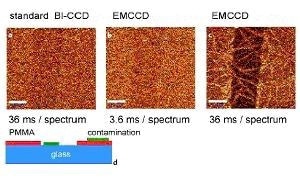
Figure 1. (a)-(c) Confocal Raman images of a 7.1 nm thin PMMA layer on glass obtained in the CH2 stretching band around 3000 / cm. Scale bar: 10 µm. (d) Schematic of the sample 30 x 50 µm, 100 x 80 pixel = 8000 spectra, 110 ms/spectrum.
To obtain the images, 200 x 200 Raman spectra were acquired in a 50 x 50 mm scan range and the intensity of the CH2 stretching band of PMMA was integrated at about 3000 / cm. Excitation power was 20 mW @532 nm using a 100x, NA=0.9 objective. Figure 1a was acquired with a normal back-illuminated (BI) CCD using a readout amplifier of 62 kHz and an integration time/spectrum of 36 ms. With a little imagination, the scratch in the middle of the image is just noticeable, but the S/N ratio is much smaller than 1.
Shown in Figure 1b is the same part of the sample imaged with an EMCCD with a gain of approximately 250. The image shows almost the same S/N, but now the integration time was just 3.6 ms, which is 10 times faster than in image 1a. For image 1a, the complete image acquisition took 25 minutes but for image 1b it took just 3.4 minutes. Figure 1c was acquired with the EMCCD, but now with the same integration time as in Figure 1a. The scratch can be seen clearly and so does the contamination in the form of a needle-like structure across the glass surface and PMMA, which will be discussed later. A sketch of the sample is shown in Figure 1d.
For the next set of images, an oil immersion objective with NA=1.4 was used and the sample was turned upside down. Integration time was 7 ms/spectrum leading to a total acquisition time of 5.4 minutes (including 0.3s/line for the back-scan). Twelve images obtained under the same conditions with different gain settings from 16 x to 1,000 x are shown in Figure 2. Again, the images were obtained by integrating the signal around the CH2 stretching band. As can be seen from the images, the S/N ratio strongly increases up to a gain setting of approximately 200 x. Above this, no more improvement in S/N is seen in the images.
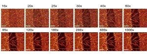
Figure 2. Comparison of confocal Raman images acquired with different settings of the EMCCD gain.
In Figure 3, the S/N ratio of the signal from the CH2 stretching band of the PMMA is plotted against the EMCCD gain. The signal’s standard deviation was taken as noise. As can be seen, the signal increases up to a gain setting of 300 x, which seems to be the optimum setting but above this value the S/N value again decreases slightly. Using the appropriate gain factor, the total improvement is more than a factor of 5.
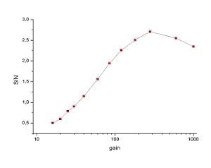
Figure 3. S/N ratio of the signal from the CH2 stretching band of PMMA plotted against the EMCCD gain.
The Identification of Contaminants
None of the spectra acquired was a pure PMMA spectrum or a pure spectrum of the contamination layer because of the limited confocal depth resolution. However, a pure glass spectrum was acquired by averaging all spectra obtained in the area of the scratch without any contamination.
Pure PMMA and contamination spectra can be calculated by subtracting the glass spectrum from the PMMA spectrum and from the spectrum of the contamination, respectively. These spectra were considered for a basis analysis, wherein each measured spectrum is fitted as a linear combination of basic spectra.
With this method, three images with the distribution of the three components (PMMA, glass, and contamination) can be achieved which were color-coded (red=PMMA, blue=glass, and green=contamination) to view their distribution (Figure 4).
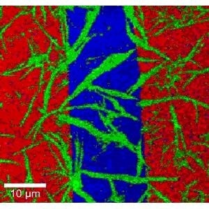
Figure 4. Color-coded confocal Raman image of a 7.1 nm PMMA layer (red) and a 4.2 nm contamination layer (green) on glass (blue). 200 x 200 spectra, 7 ms integration time/spectrum. Total acquisition time 5.4 minutes.
The spectra of the different components are shown in Figure 5. For better comparison, they are shown with identical maximum intensities. With respect to the glass spectrum, the PMMA spectrum is amplified approximately 20 times and the contamination spectrum is amplified about 15 times.
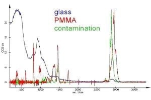
Figure 5. Raman spectra as calculated from the Raman measurement in Figure 4, displayed with identical maximum intensities. The scale is only correct for PMMA. The PMMA spectrum is amplified about 20 times and the contamination spectrum about 15 times with respect to the glass spectrum.
From this, the green spectrum (contamination) can be easily recognized as an alkane. To investigate the AFM thickness, the sample was prepared a few weeks before the Raman measurement and kept in a polystyrene (PS) container. The PS container is produced by injection molding and the mold is coated with alkane for better separation. Since the sample was stored (maybe in a warm environment), part of the alkane evaporates and condenses on the sample, which explains the needle-like structure and the fact that the scratch is covered by coating.
The scale given in Figure 5 is correct for PMMA, revealing a maximum of just 28 counts. The signal averaged over the complete CH2 stretching regime (about 150 pixels or 330 / cm) is 1965 counts. The EM gain for this measurement was approximately 600 x, and therefore the 1965 counts correspond to just 1.4 photons maximum per CCD pixel and 99 electrons (110 photons) total! However, how to acquire a good Raman spectrum with so few electrons? The reason is that approximately 20,000 spectra were averaged to measure the PMMA spectrum depicted in Figure 5. Therefore, the overall signal is 20,000 times greater.
Conversely, only those spectra were acquired where PMMA was present. For this, the signal per spectrum must be sufficiently strong to show the PMMA distribution in the Raman image, as this will make it easy to choose the right spectra for the averaging. As can be observed, 1.4 photons per EMCCD pixel are sufficient to view the distribution of the PMMA layer in this case and to select the correct spectra for the averaging process.
If a substrate without any background signal in the CH2 stretching regime has been used, then the result would have been even more impressive. The three spectra of PMMA, glass, and alkane with identical intensity scale are shown in Figure 6.
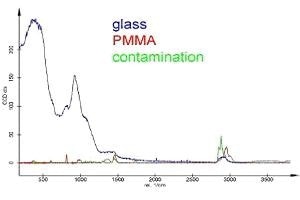
Figure 6. Same spectra as in Fig. 5 but with correct scale.
As can be seen, the glass substrate used has a small Raman peak with about one third of the alkane signal and about half of the signal of PMMA in exactly this area. It is clear that the confocality of the Raman system is important for the detectibility of thin layers. Even with the most appropriate confocal setup, the information depth is no less than 500 nm, meaning 500 nm of glass contributes to the Raman signal. Since the Raman signal is proportional to the amount of material, a typical (non-confocal) setup would have collected a glass signal that is over 300 times higher (170 µm cover glass thickness), making it impossible to detect the thin coating layers even with relatively longer integration times.
Summary
It was shown that the use of an EMCCD camera can significantly increase speed and detection efficiency, particularly for the short integration times required with a confocal Raman microscope. The distribution of a 7.1 nm PMMA and a 4.2 nm alkane layer on a glass substrate can be easily detected and identified with an integration time of just 7 ms for each spectrum, reducing the overall acquisition time to 5.4 minutes for a 200 x 200 (= 40,000) spectra confocal Raman image.
In the case of extremely small signals that are dominated by the readout noise of the CCD, the use of an EMCCD camera can enhance the S/N ratio by a factor of 5 - 10 when compared to the best available standard CCDs. For larger signals, the electron multiplying circuit can be simply switched off and all properties of a normal (back-illuminated) CCD are maintained.

This information has been sourced, reviewed and adapted from materials provided by WITec GmbH.
For more information on this source, please visit WITec GmbH.