In the past decade, Group III-nitride materials have been widely used for visible and ultraviolet light emitting diodes and blue, violet laser diodes. Most of these optoelectronic devices are typically fabricated on the conventional polar (0001) c-plane oriented substrate materials. Devices grown on the polar substrate orientation suffer undesirable spontaneous and piezoelectric polarization resulting in significant band bending in the quantum well. This reduces radiative recombination efficiency and lowers device performance.
Now the technical team at Oxford Instruments-TDI, led by Dr. Alexander Usikov, has made significant progress in solving this problem, and is working closely with a leading LED manufacturer to fabricate these semi-polar GaN layer for optoelectronic devices. This would increase radiative recombination efficiency and device performance.
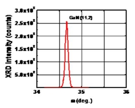
In order to diminish these polarization effects, growth of GaN-related devices along semi-polar and non-polar directions has been studied intensely. Using hydride vapour phase epitaxy (HVPE), the team has grown high quality, semi-polar (11.2) oriented GaN on (10.0) m-plane sapphire with an intermediate layer between the sapphire substrate and the GaN layer.
The semi-polar (11.2) GaN layers were grown in the temperature range from 930 to 1050oC in an inert argon ambient at atmospheric pressure. Gallium and aluminum were used as metallic source materials and hydrogen chloride (HCl) and ammonia (NH3) as the active gases for the HVPE process. The epitaxial growth of GaN was performed at approximately 60m/per hour using an intermediate layer deposited on m-plane sapphire followed by an undoped GaN layer. The growth procedure results in high quality, semi-polar GaN layer with thickness up to 30 µm.