Image showing the differences along the edge of the graphene.
Courtesy of NPL Managment Ltd.
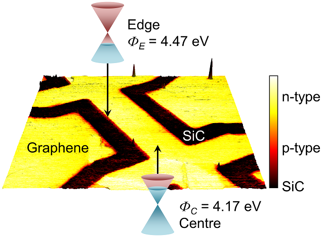
NPL scientists have made an interesting discovery that graphene devices exhibit a different conductivity at the center when compared to their edges.
Epitaxial graphene’s local nanoscale electronic properties, focussing on variations between central parts and edges of graphene Hall bar devices, were studied using local scanning electrical techniques.
The edges of the graphene channel showed hole conduction (p-doped), whereas the central parts showed electron conduction (n-doped). Using side-gates, conduction was accurately tuned along the edges of the graphene devices, but the conductive properties remained unaffected at the center.
As the semiconductor industry continues to relentlessly push the physical size of devices down to tens of nanometres, non-uniform conductivity across the graphene can lead to a significant variation in the device performance.
Dr. Olga Kazakova - Principal Research Scientist at NPL
These effects become more severe at a micro scale and nearly 25% of the material is affected by the altered properties at the nano scale.
Even though both p- and n-type semiconductors are conductors, it is important to acknowledge different types of conduction while manufacturing electronic devices.
Considering the ever-increasing use of graphene in the electronics industry, these differences will need to be accommodated by new devices.
Dr. Olga Kazakova, Principal Research Scientist at NPL, spoke exclusively to AZoM.com about the implications that this difference in conductivity has on the semiconductor industry, "as the semiconductor industry continues to relentlessly push the physical size of devices down to tens of nanometres, non-uniform conductivity across the graphene can lead to a significant variation in the device performance," she continues to say "this huge change in conductivity must be fully understood and controlled for a stable device performance, in particular where the interaction with environment is envisaged (e.g. sensors)."
It was observed that the inversion effects were the highest immediately after cleaning graphene.
This proved that the carrier inversion was the result of the defects introduced at the channel edge during the plasma etching process employed in the fabrication of the graphene devices. Reduction in the inversion effects was observed after a few hours due to adsorption of airborne molecules onto the uncoupled bonds at the edges of the devices.
Dr. Kazakova said "the carrier inversion observed at the graphene edges forms parallel conduction channels consisting of electrons and holes as well as essentially carrier-free localised areas. Such effects have previously never been observed in conventional semiconductor devices. This phenomenon could lead to entirely new types of devices that are yet to be discovered."
The study results are helpful to develop graphene nanoribbon devices and explore the quantum Hall effect and edge photocurrents. The group are now exploring these effects in different types of graphene for comparison and seeking to understand the cause of these effects better.