Jun 30 2015
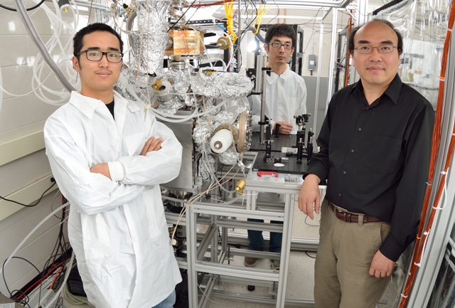 (l-r) Faran Zhou, physics and astronomy doctoral student; Terry Han, who just earned his Ph.D. in physics and astronomy; and Chong-Yu Ruan, associate professor of physics and astronomy. They are part of a team that developed an ultrafast microscope that allows researchers to view changes in materials caused by laser pulses. Photo by Harley Seeley.
Researchers at Michigan State University have developed an ultrafast electron-based imaging technique that makes it possible to modify the electronic properties of materials such that easy transmission of an electrical current is made possible.
The study, published in the journal Science Advances, can pave the way for designing new and enhanced semiconductors. A semiconductor is a kind of material, which conducts electricity under certain conditions but does not do so in other conditions. This makes it an excellent medium to regulate electrical current and hence is used in a wide range of electronics, including PCs.
The electrical properties of this substance largely rely on dopants, which are trace impurity elements. When these impurities are adequately added to the material, highly efficient solid-state electronics can be developed.
The researchers observed that when an ultrafast laser pulse is shot into the material, the properties of the material changes as if it had been doped chemically. This procedure is referred to as photo-doping.
"The material we studied is an unconventional semiconductor made of alternating atomically thin layers of metals and insulators. This combination allows many unusual properties, including highly resistive and also superconducting behaviors to emerge, especially when ‘doped’," said Chong-Yu Ruan, who headed the study at MSUand serves as an associate professor of physics and astronomy.
The electron-based imaging method developed by the MSU researchers enabled them to view the modifications in the materials. Upon changing the intensities and wavelengths of the laser pulses, the team was able to view the phases having a range of properties, recorded on the femtosecond timescale. A femtosecond is one quadrillionth of a second.
"The laser pulses act like dopants that temporarily weaken the glue that binds charges and ions together in the materials at a speed that is ultrafast and allow new electronic phases to spontaneously form to engineer new properties. Capturing these processes in the act allows us to understand the physical nature of transformations at the most fundamental level, said Ruan. Ultrafast photo-doping has potential applications that could lead to the development of next-generation electronic materials and possibly optically controlled switching devices employing undoped semiconductor materials," said Philip Duxbury, a team member and chairperson of the Department of Physics and Astronomy.