Berkeley Lab Team Creates 2D Atomically Thin Perovskite Hybrid Nanostructures from Ionic Materials

Atomically thin 2D sheets of conducting perovskite hybrids have been produced in solution. The crystals have conducting properties that make them a contender as a replacement for silicon.

Ultrathin sheets of a new 2D hybrid perovskite are square-shaped and relatively large in area.

The 2D sheets were produced by Researchers at the U.S. Department of Energy (DOE)’s Lawrence Berkeley National Laboratory (Berkeley Lab). As their structure is ionic, rather than covalent, they possess efficient color-tunability, photoluminescence, and a distinct structural relaxation that has not been observed in covalent semiconductor sheets. The atomically thin sheets of perovskite have a square shape, large area, and are of high quality.

The 2D hybrid organic-inorganic perovskite sheets have joined the list of potential replacements for silicon which includes graphene, molybdenum disulfide and boron nitride.

We believe this is the first example of 2D atomically thin nanostructures made from ionic materials                          

                                                              - Dr. Peidong Yang, Berkeley

Dr. Peidong Yang, a chemist with Berkeley Lab’s Materials Sciences Division and world authority on nanostructures, first came up with the idea for this research some 20 years ago. Yang is a co-director of the Kavli Energy NanoScience Institute (Kavli-ENSI), and holds appointments with the University of California (UC) Berkeley.

The results of our study open up opportunities for fundamental research on the synthesis and characterization of atomically thin 2D hybrid perovskites and introduces a new family of 2D solution-processed semiconductors for nanoscale optoelectronic devices, such as field effect transistors and photodetectors.                                        

                                                              - Dr. Peidong Yang, Berkeley


Conventional perovskites are metal-oxide ionic materials that possess properties such as superconductivity, magnetoresistance, piezoelectricity and ferroelectricity.

Organic-inorganic hybrid perovskites that have been converted into crystals or thin films by solution-processing have been used for photovoltaic devices. These PV devices have until now reached an efficiency of 20%.

Techniques such as mechanical exfoliation, chemical vapor deposition and spin-coating have not been very effective for separating perovskites into separate 2D sheets.

When Yang was a PhD student at Harvard University, he had suggested a new method for creating 2D hybrid perovskite nanostructures and modifying their electronic properties. He passed on this idea to Letian Dou, a post-doctoral student in his research group, and co-lead author of the paper.
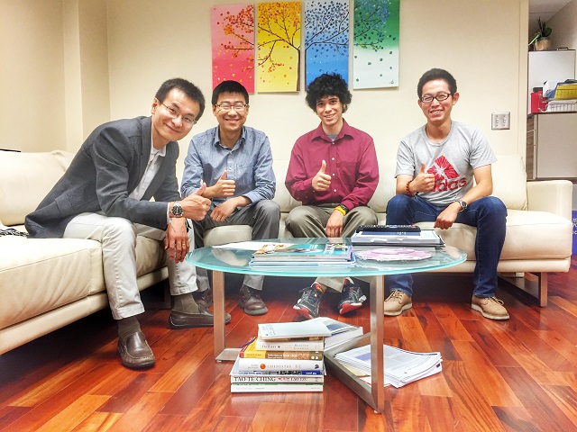
Dou collaborated with Andrew Wong and Yi Yu, other lead authors of the paper, and synthesized free-standing 2D sheets of a hybrid perovskite - CH3NH3PbI3, which is made up of carbon, nitrogen, hydrogen. lead and iodine atoms.

“Unlike exfoliation and chemical vapor deposition methods, which normally produce relatively thick perovskite plates, we were able to grow uniform square-shaped 2D crystals on a flat substrate with high yield and excellent reproducibility,” says Dou. “We characterized the structure and composition of individual 2D crystals using a variety of techniques and found they have a slightly shifted band-edge emission that could be attributed to structural relaxation. A preliminary photoluminescence study indicates a band-edge emission at 453 nanometers, which is red-shifted slightly as compared to bulk crystals. This suggests that color-tuning could be achieved in these 2D hybrid perovskites by changing sheet thickness as well as composition via the synthesis of related materials.”

                                                             - Dr. Peidong Yang, Berkeley

The high crystallinity quality is demonstrated by geometry of the square-shaped 2D crystals, and as they are large in size, they would possibly be easy to integrate in next-generation devices.

The study paper, titled “Atomically thin two-dimensional organic-inorganic hybrid perovskites,” has been published in the journal, Science.

The DOE’s Office of Science supported the study. The characterization work was performed at beamline 7.3.3 of the Advanced Light Source and Molecular Foundry’s National Center for Electron Microscopy.

Jake Wilkinson

Written by

Jake Wilkinson

Jake graduated from the University of Manchester with an integrated masters in Chemistry with honours. Due to his two left hands the practical side of science never appealed to him, instead he focused his studies on the field of science communication. His degree, combined with his previous experience in the promotion and marketing of events, meant a career in science marketing was a no-brainer. In his spare time Jake enjoys keeping up with new music, reading anything he can get his hands on and going on the occasional run.

Citations

Please use one of the following formats to cite this article in your essay, paper or report:

  • APA

    Wilkinson, Jake. (2019, February 08). Berkeley Lab Team Creates 2D Atomically Thin Perovskite Hybrid Nanostructures from Ionic Materials. AZoM. Retrieved on April 28, 2024 from https://www.azom.com/news.aspx?newsID=44577.

  • MLA

    Wilkinson, Jake. "Berkeley Lab Team Creates 2D Atomically Thin Perovskite Hybrid Nanostructures from Ionic Materials". AZoM. 28 April 2024. <https://www.azom.com/news.aspx?newsID=44577>.

  • Chicago

    Wilkinson, Jake. "Berkeley Lab Team Creates 2D Atomically Thin Perovskite Hybrid Nanostructures from Ionic Materials". AZoM. https://www.azom.com/news.aspx?newsID=44577. (accessed April 28, 2024).

  • Harvard

    Wilkinson, Jake. 2019. Berkeley Lab Team Creates 2D Atomically Thin Perovskite Hybrid Nanostructures from Ionic Materials. AZoM, viewed 28 April 2024, https://www.azom.com/news.aspx?newsID=44577.

Tell Us What You Think

Do you have a review, update or anything you would like to add to this news story?

Leave your feedback
Your comment type
Submit

While we only use edited and approved content for Azthena answers, it may on occasions provide incorrect responses. Please confirm any data provided with the related suppliers or authors. We do not provide medical advice, if you search for medical information you must always consult a medical professional before acting on any information provided.

Your questions, but not your email details will be shared with OpenAI and retained for 30 days in accordance with their privacy principles.

Please do not ask questions that use sensitive or confidential information.

Read the full Terms & Conditions.