Feb 6 2017
A technique developed by materials researchers at UC Santa Barbara (UCSB) is seen as a way to enable the efficient design and manufacture of organic circuitry with varying levels of complexity, but which uses the same semiconductor material.
 Credit: Sonia Fernandez
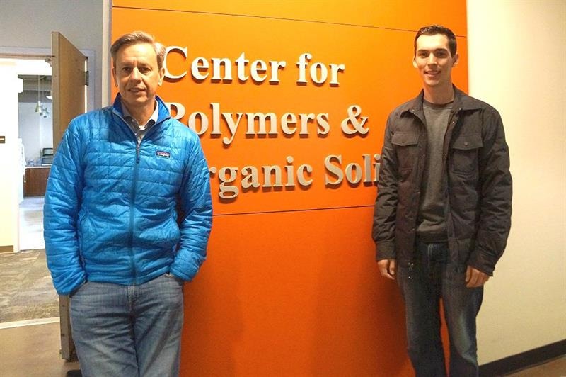
“It’s a different strategy by which you can take a material and change its properties,” said Professor Guillermo Bazan, pictured left. The team says that, by adding fullerene or copper tetrabenzoporphyrin (CuBP) molecules in strategic places, the charge carriers in semiconducting materials may be controlled and inverted, not only bringing better device performance, but also more economical manufacture.
Polymer semiconductors depend on the movement of charge carriers across the material. While high-mobility, high-performance materials have been developed, the team says fine control of electrons and holes will allow sophisticated polymers to reach their full potential.
Researcher Michael Ford, pictured right, noted: “There’s been a large effort to make new materials, but a lot of them may not be appropriate in conventional low-power devices.” Many of these materials exhibit ‘ambipolar’ conduction, meaning they transport negative and positive charges. However, when only a certain charge is required, the opposite charge diminishes the material’s performance. “They’re always ‘on’, so you always have a current running through the device,” Ford said.
The UCSB development was, apparently, an accidental discovery. While investigating the properties of two materials, Ford saw the use of fullerenes limited conduction of electrons, while allowing holes to remain mobile.
“I noticed it solved the problem with my other material never turning off,” Ford said. He decided to employ the fullerene additive from one experiment to address issues in the other and found it could allow only positive charges to move, while adding operational stability.
From there, the team worked to control negative charge conduction in the same way. CuBP was introduced, which turned off ambipolar transport in the opposite way from the fullerene.
“We had two devices, both using the same polymer semiconductor but with different additives,” Ford explained. “One was a switch for holes, the other was a switch for electrons. This enabled us to develop a complementary inverter.”
“We have, for the first time, this ability to take ambipolar semiconductors and design a circuit in certain parts of which only electrons move or only holes are moving,” said Prof Bazan, “but keep the same semiconductor material.”
According to the team, the approach may have application in low-cost, low-power flexible electronics. “It’s this idea where we can have an additive that can be a small fraction of the total and which will allow us to master the electronic properties of the semiconductor,” Prof Bazan concluded. “Once you have that under control, you can do all sorts of cool things.”
Source: http://www.ucsb.edu/