Sponsored by HORIBAOct 24 2013
Laser processing offers a quick, non-contact and flexible method of modifying and patterning materials, from glasses to metals. Glasses, or more generally, optical materials, may react to laser irradiation by changing their refractive index. This effect has been used successfully for creating 3D structures in bulk glass.
Photo-Structural Changes Induced by Laser Irradiation
Laser processing mostly results in photo-structural changes either during ablation or the more subtle modification of the refractive index. Raman spectroscopy is very useful in understanding the photo-structural changes underlying the processing.
In Arsenic sulfide (As2S3)
Arsenic sulfide is part of the chalcogenide glass family, which exhibits several interesting properties that can be exploited for the fabrication of photonic devices. Specifically, their high infrared transparency, large nonlinear refractive indices and low phonon energies make them good candidates for use in the fabrication of all-optical switches and as integrated optical elements.
The Raman spectrum of vitreous As2S3 is dominated by the strong band at ~345 cm-1 attributed to the symmetric stretching vibrational mode of AsS3/2 pyramids. Besides this strong band, there are additional features (shoulders) at approximately 310 and 380 cm-1, which are assigned to the asymmetric stretching modes of AsS3/2 pyramids and As–S–As bridges, respectively.
The presence of sulphur in excess in the thin film form is indicated by the weak band at 485–495 cm-1 associated with the S–S stretching vibration in S8 rings. Weak bands situated at 188 cm-1 and 235 cm-1 can be attributed to the bending modes of AsS3/2 pyramids, S8 and As4S4 molecules. Ideally, the spectrum should only consist of the strong band at 345 m-1.
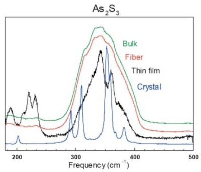
Figure 1. Raman spectrum of As2S3 in bulk, fiber, thin film and crystal form
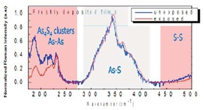
Figure 2. Comparison between the Raman spectrum of arsenic trisulfide unexposed (blue curve) and exposed to the laser (red curve)
The presence of the additional structures mentioned above is due to the formation of “wrong bonds” in the glass network. This is particularly visible in the thin film form (Figure 1), where As4S4 molecular clusters and As-As homopolar bonds are created during the deposition process.
After irradiation, the peaks at the low wavenumbers, corresponding to the presence of As4S4 molecules, show a significant decrease in intensity as shown in Figure 2. This is interpreted as a decrease in the content of As4S4, due to the photosynthetic reaction whereby the original stoichiometry is recreated, partially reforming the As2S3 network according to:
As4S4 + S2 2 As2S3
Concurrently, the relative intensity of the peak at 235 cm-1, linked to the presence of As-As homopolar bonds, exhibits a relative increase, due to the photolytic reaction whereby As-S heteropolar bonds decompose to yield “wrong” homopolar bonds, according to:
2 As-S As-As + S-S
In Silicon Oxide (SiO2)
Raman spectroscopy has been proved as an efficient method for characterizing structural modification in fused silica. The key feature of the spectrum of fused silica is the broad band centered at around 440 cm- 1, attributed to the Si-O-Si bond rocking and bending in SiO4 tetrahedra.
The two smaller bands at 490 cm-1 (D1) and 606 cm-1 (D2) have been attributed to three- and four-member siloxane rings, respectively, in the silica network. Comparing these spectra between pristine and irradiated samples as shown in Figure 3 reveals two principle trends as the pulse energy is increased:
- The amplitude of both defect lines D1 and D2 increases
- The width of the main band at 440 cm-1 decreases.
The increased amplitude of the D1 and D2 defect peaks is attributed to the change in ring statistics here six-fold rings transform to three-fold and four- fold rings upon laser radiation.
In the case of β irradiation, the narrowing of the main 440 cm- 1 band with increasing irradiation energy has also been reported. This band frequency relates to the Si-O-Si angle in the glass network, and its width reflects the distribution of the Si-O-Si angle. The narrowing of the 440 cm-1 band can hence be explained by photoinduced ruptures of the strained Si-O-Si bridging bonds which are more likely to break than unstrained bonds.
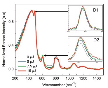
Figure 3. Raman spectra of pristine and fs IR laser-irradiated fused silica with increasing laser pulse energies. The insets are magnified images of the D1 and D2 lines at 490 cm-1 and 606 cm-1, respectively.
3D Waveguide Writing in Bulk Glass
A femtosecond Ti:Sapphire laser is focused inside a bulk glass sample. A motorized stage is used to move the sample and the refractive index is modified at the laser focus along the path followed by the stage as shown in Figure 4.
In case the refractive index change is positive, a waveguide is created as shown in Figure 4, much like an optical fiber embedded inside the glass sample. This lays the ground for producing 3-D optical circuits.
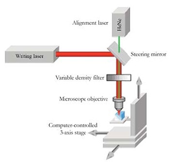
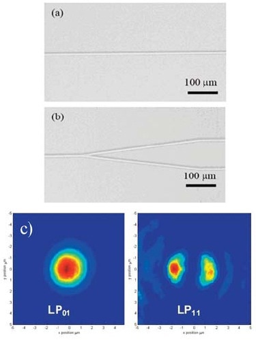
Figure 4. Optical microscope images of (a) a single channel waveguide, (b) a Y coupler, and (c) near-field intensity profile of the LP01 and LP11 modes in a single- channel waveguide

This information has been sourced, reviewed and adapted from materials provided by HORIBA.
For more information on this source, please visit HORIBA.