Additive manufacturing (AM), or 3D printing, is the process by which a solid object is built layer by layer from a digital model. This process provides advantages over traditional manufacturing techniques in a number of ways, including material, time, and cost savings. It has the potential to produce near-net-shape metallic components across various markets including medical devices, automotive, and aerospace.

Figure 1. EBSD is an alternative characterization technique that provides a comprehensive characterization of AM materials.
However, a final 3D printed output with the same shape as a product fabricated by traditional methods is not enough for these challenging applications. They must also have material properties equal to or superior to their traditionally processed counterparts. Optimizing the deposition parameters of the AM process and any subsequent thermal processing is important for obtaining the desired material properties.
Limitations of Existing Solutions
Processing parameters of additive manufacturing and any subsequent thermal processes are adjusted to alter the microstructure of the material and to acquire the properties needed to meet the requirements of high-performance applications. There are a number of techniques available to characterize the microstructures of these components, which are outlined below.
Light Optical Microscopy (LOM) is able to deliver qualitative information on the size and shape of grains through grain boundary contrast imaging. However, due to the involvement of rapid cooling in the AM process, the grain size is typically too small to be resolved accurately with LOM.
The images acquired by scanning electron microscopy (SEM) provide grain size data with improved spatial resolution. However, SEM yields limited data on the distribution of phases present in the AM microstructure, especially for polymorph phases involving crystallographic structure changes but with no change in chemistry - one example being HCP-Ti vs BCC-Ti.
Information on the local phase distribution and the orientation relationships that develop in the event of phase transformations can be obtained with transmission electron microscopy (TEM). However, TEM has a limited analysis area and often involves the manual determination of phase and orientation relationships, therefore limiting the number of quantitative measurements that can be performed.
X-ray diffraction (XRD) can provide data on the phase fraction present and the preferred orientation developed during AM. However, since XRD is a bulk-measurement method, information on the spatial distribution of the data cannot be obtained. As AM is a layer-by-layer manufacturing process, it is important to have spatial information in order to understand any variations that develop during the process.
Electron Backscattered Diffraction (EBSD)
An alternative characterization technique is electron backscattered diffraction (EBSD), which is capable of performing a comprehensive characterization of AM materials (Figure 1). EBSD is advantageous in many ways – for example, direct measurement of grain size and shape via discrete crystallographic orientation measurements, with nanometer-scale spatial resolution, eliminates grain boundary contrast errors. Also, measurements of the grain shape and size can be carried out after solidification and after any subsequent thermal processing.
EBSD provides direct phase identification and spatial mapping of phase distributions. The AM process involves heating, melting, and rapid solidification of metals. Phase transformations can occur as a result of this thermal processing and therefore controlling these transformations is crucial to obtain the material properties desired.
EBSD characterizes AM materials automatically and rapidly, thus allowing for fine spatial resolution, large area data collection, and statistically accurate analysis. Therefore, local variations become more relevant and meaningful.
Microstructure and local orientations can be directly correlated with the actual stresses within a material, due to the ability of EBSD to perform direct measurement of crystallographic orientation along with the spatial distribution of these orientations.
Microanalysis Results
Many different AM methods are available, depending on the starting material used. Rod-based methods include shaped metal deposition (SMD) and fused deposition modeling (FDM), and powder-based methods include selective laser sintering (SLM) and electron beam melting (EBM).
Each of these approaches involves heating of the starting material for controlled deposition and subsequent cooling for solidifying the structure into the desired shape. The microstructure and mechanical properties of the AM materials are determined by the heating and cooling profiles.
The characterization capabilities of EBSD are demonstrated by collecting data using APEXTM Software for EBSD from a titanium sample fabricated by SLM. In this process, the powdered titanium is locally melted and sintered together using a focused laser beam to construct the 3D structure. An EBSD orientation map is presented in Figure 2, showing colors corresponding to the crystallographic planes oriented along the deposition axis.
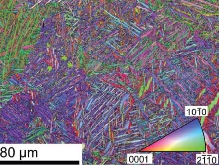
Figure 2. EBSD orientation map across the cross-section of selective laser melting (SLM) deposited titanium showing lath and packet microstructure with no significant preferred orientation.
The microstructure is composed of small needle-shaped grains distributed within ‘packets’, which show the prior beta phase grain size. The beta phase has not been retained and only alpha phase titanium was detected. No significant preferred orientation was detected during this analysis, suggesting the absence of significant solidification textures developing during manufacturing. Columnar grains with a stronger texture were detected in similar materials fabricated by wire-fed approaches.
A grain map is presented in Figure 3, where the size and shape of the grains are characterized by random colors. From this region, assuming a circular grain, analysis of more than 30,000 grains with an average grain size of 740nm has been sampled. Since the shape of the grains is clearly not circular, a grain area metric with a value of 0.794µm2 is derived for this microstructure. This value more accurately represents the true grain structure. A few anomalous larger grains are shown in the lower-right analysis region.
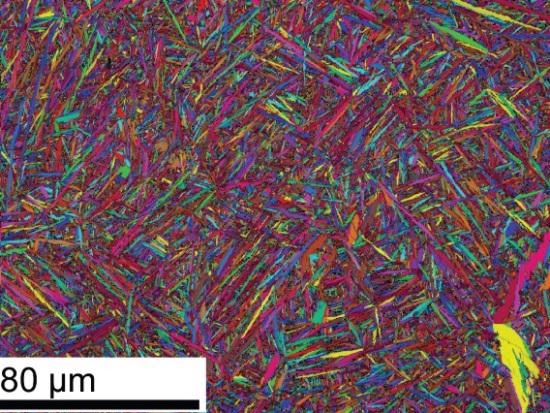
Figure 3. EBSD grain map from SLM deposited titanium where detected grains are randomly colored to showcase size and morphology.
These measurements provide information on grain size and shape, grain shape orientation, grain shape aspect ratio, and crystallographic correlations. These can be significant in the analysis of the solidification microstructures developing during the AM process and the changes that can happen during subsequent thermal processing.
An orientation map from a 316L stainless steel sample is depicted in Figure 4. The sample was fabricated by locally binding metallic powder in three dimensions, followed by sintering the structure at high temperatures. The grain size was considerably bigger with this material and process (15µm). As with the previous method, no significant preferred orientation was identified, and only FCC austenite was observed.
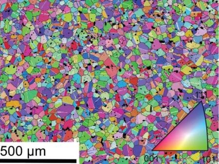
Figure 4. EBSD orientation map from 3-D printed and sintered 316L stainless steel sample where identified twin boundaries are colored white and random grain boundaries colored black.
In both cases, the possible phases are structurally different but chemically similar. Therefore, EBSD is ideal for phase analysis. Figure 3 shows a significant fraction of twin boundaries as white lines. The final material properties such as yield strength or corrosion resistance can be influenced by these special boundaries. This image also shows porosity as larger black regions within the microstructure, which can be related to the deposition parameters employed.
Conclusion
Using the Pegasus Analysis Systems is recommended to facilitate the development and optimization of AM processes creating homogenous, high-performance metallic parts for the medical device, automotive, and aerospace markets.
Pegasus Analysis Systems perform integrated EDS and EBSD characterization with a user-friendly interface to rapidly and reliably analyze grain shape and size, composition, grain orientation, and preferred orientation, and phase distribution.
With EDAX EBSD detectors, rapid, sensitive, and smart EBSD pattern collection with unprecedented indexing rates and orientation precision can be obtained to analyze the complex microstructures developing during AM processes.

This information has been sourced, reviewed and adapted from materials provided by Gatan Inc.
For more information on this source, please visit Gatan Inc.