The significance of the entrance slit and the diffraction grating in forming a spectral image of the incident light in the image plane is discussed in the articles “An Introduction to a Spectrometer: The Slit” and “An Introduction to a Spectrometer: Diffraction Grating.”
In traditional spectrometer (monochrometer) designs, a second slit is located in the image plane, called the exit slit. Usually, this exit slit the same size as the entrance slit, given that the width of the entrance slit is one of the limiting factors on the spectrometer’s resolution.
In this configuration, an element detector is positioned behind the exit slit and this is followed by rotating the grating to scan the spectral image across the slit. Thus, the intensity of the light is measured as a function of wavelength.
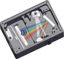
In modern spectrometers, linear detector and CCD arrays have enabled the development of “fixed grating” spectrometers. When the pixels across the CCD are hit by the incident light, each pixel represents a part of the spectrum that the electronics can translate and display with a given intensity using software.
This development has made it possible to construct spectrometers without any moving parts, considerably reducing the size and power consumption. Compact multi-element detectors have enabled the development of a new class of low-cost, compact spectrometers that are generally known as “miniature spectrometers.”
Detector Types
Although there are different ways to characterize photodetectors, the most significant differentiator is the detector material. Si and InGaAs are the two most common semiconductor materials employed in miniature spectrometers.
When designing a spectrometer, it is important to choose the right detector material because the upper wavelength limit (λmax) is detected by the bandgap energy (Egap) of the semiconductor. λmax can be detected by the relationship given below:
Where, c is the speed of light and h is Plank’s constant.
The speed of light and the product of Plank’s constant can be expressed as 1.24 eV•µm or 1240 eV•nm to simplify the conversion of energy into wavelength. For instance, Si’s bandgap energy is 1.11 eV which corresponds to the maximum wavelength of 1117.117 nm.
On the other hand, InGaAs is an alloy formed by mixing InAs and GaAs, which have respective bandgap energies of 0.36 eV and 1.43 eV. The bandgap energy, based on In and Ga ratios, can be tuned in between those two values.
However, not all ratios of In and Ga can be easily fabricated due to various factors and, therefore the standard configuration for InGaAs detector arrays is 1.7 µm (or 0.73 eV). Extended InGaAs arrays can also be used, which can detect out to 2.6 µm or 2.2 µm, but these detectors are not only more expensive, but also noisier than conventional InGaAs detectors.
It is slightly harder to quantify the lower detection limit of a material, because it is determined by the absorbance characteristics of the semiconductor material, and can differ widely with the detector thickness.
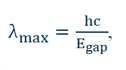
The detection limit of the detector can also be lowered by placing a fluorescent coating on the window of the detector, which will then absorb the higher energy photons and reemit lower energy photons, which are subsequently detected by the sensor. A comparison of the detectivity (D*) as a function of wavelength for both InGaAs and Si (CCD), is shown in Figure 1.
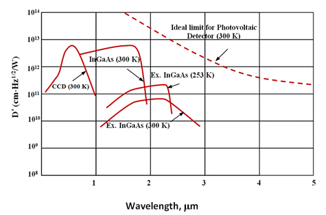
Figure 1. Approximate D* values as a function of wavelength for some typical detectors
CCDs, BT-CCDs, and PDAs
Currently, InGaAs detector arrays are only available in one configuration, but Si multi-element detectors are available in three different subcategories - back-thinned charge coupled devices (BT-CCDs), charge coupled devices (CCDs), and photodiode arrays (PDAs).
CCD technology enables the construction of small pixel size (~14 µm) detectors as it removes the requirement of direct readout circuitry from individual pixels. To achieve this, the charge is transferred from one pixel to another, enabling all of the information along the array to be read out from one pixel.
CCDs are an ideal option for most miniature spectrometers, as they can be designed quite inexpensively. However, they come with two disadvantages; first, the gate structure located on the front of the CCD can make the incident light scatter, which means it won't be absorbed, and second, a relatively large P-Si substrate is required by CCDs to ease low cost production, but this also limits the detector’s efficiency (particularly at shorter wavelengths) as a result of absorption through the Player.
BT-CCDs provide the ideal option to mitigate these problems in spectroscopy applications where very high sensitivity is required. BT-CCDs are designed by etching the CCD’s P-Si substrate to a thickness of about 10 µm. This process not only reduces the amount of absorption, but also increases the detector’s overall efficiency.
In addition, the detector is also illuminated from the back side (P-Si region), removing the effects from the gate structure on the detector surface. Figure 2 depicts a typical comparison of the quantum efficiency between a back-illuminated BT-CCD and a traditional front-illuminated CCD.
Figure 2. Typical quantum efficiency of front-illuminated CCD and back-illuminated CCD
While the use of BT-CCDs in spectroscopy provides clear benefits, there are two key drawbacks that should be taken into account. First, this process considerably increases the production cost, and second (as the detector is very thin) an etaloning effect can be caused by reflections off the front and back surfaces of the detector.
Although the etaloning effect associated with BT-CCDs can be mitigated by a deep depletion process, this will again increase the cost of the production process.
PDA detectors are more conventional linear detectors that contain a set of individual photodiodes arranged in a linear fashion using CMOS technology. While PDA detectors lack high sensitivity and small pixel size, they provide several benefits compared to BT-CCD and CCD detectors.
First, the absence of charge transfer removes the requirement for a gate structure on the front surface of the detector, and considerably increases the readout speed. Second, the well depth of a PDA detector is relatively higher than the well depth of a CCD - the well depth of a typical PDA detector is ~156,000,000e- compared to ~65,000e- for a typical CCD.
Due to the larger well depth, PDA detectors have an extremely linear response and a very large dynamic range ~50,000:1. These properties make these detectors suitable for applications where small changes in large signals, such as LED monitoring need to be detected.
Overview
Different types of detectors and the role they play in miniature spectrometers were discussed in the previous sections. However, noise sources are also equally important and no discussion of detectors will be complete without covering these factors and how they can be mitigated with TE Cooling.
Detector Noise
Readout noise, fixed pattern noise, dark noise, and shot noise are the main sources of noise found in an array detector.
Readout noise is caused by electronic noise in the detector output stage and associated circuitry, which mainly dictates the spectrometer’s detection limit.
Shot noise is associated with the statistical variation in the number of photons incident on the detector, which follows a Poisson distribution. As a result, shot noise is proportional to the square root of the incident photon flux.
Dark noise is related to the statistical variation in the number of electrons produced in a dark state. Even when no incident light is present, a photo detector exhibits a small output. This is called the dark output or dark current.
Dark current strongly relies on ambient temperatures and is caused by thermally generated electron movements. Dark noise, similar to shot noise, also follows a Poisson distribution; therefore, dark noise is proportional to the square root of the dark current.
The fixed pattern noise is the variation in photo-response between adjacent pixels. This variation largely results from variations in the quantum efficiency among pixels caused by non-uniformities in the film thickness and aperture area that occur during fabrication.
The total noise of an array detector is the root square sum of these four noise sources.
TE Cooling
An effective way to reduce dark noise and improve the dynamic range and detection limit is by cooling an array detector with a built-in thermoelectric cooler (TEC). For Si detectors, dark current halves when the temperature decreases by about 5 to 7 °C and doubles when the temperature increases by about 5 to 7 °C.
Figure 3 illustrates the dark noise for a cooled and un-cooled CCD detector at an integration time of 60 seconds. When operating at room temperature, the dark noise almost saturates the un-cooled CCD. When the CCD is TEC-cooled to only 10 °C, the dark noise is reduced by about two times and the dark current is reduced by about four times. This makes the CCD to operate at a longer integration time for detecting weak optical signals.
When a CCD-based spectrometer is used in non-demanding high light level applications such as LED measurement, the reduced dark noise caused by TE cooling is minimal due to the relatively short integration time used.
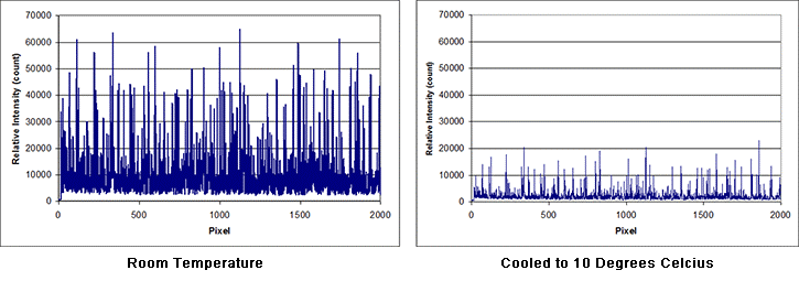
Figure 3. Dark current for cooled and un-cooled CCD detector (integration time = 60 s)
As a rule of thumb, the detector operates in a read noise limited state when the integration time of a CCD spectrometer is set to less than 200 ms. As a result, no major noise reduction occurs due to the TE cooling; although the temperature regulation under these conditions will be advantageous for long-term baseline stability.

This information has been sourced, reviewed and adapted from materials provided by B&W Tek.
For more information on this source, please visit B&W Tek.