The innovative Symmetry CMOS-based EBSD detector, together with the powerful AZtec® software is capable of obtaining EDS and EBSD data at speeds in excess of 3000 indexed patterns per second (pps).
These speeds are twice as fast as those that can be achieved with conventional CCD-based detectors, and are further improved by the fact that extreme pixel-binning of the diffraction patterns is not needed. This highlights that the quality of the data gathered using the Symmetry detector is considerably better than with CCD-based detectors, both in terms of angular accuracy and hit rate.
This article supplies examples explaining how the Symmetry CMOS-based EBSD detector can be used to characterize the microstructures in two example metals at high speeds, offering reliable statistics in affordable timescales.
Results
Two different samples were analyzed using the Symmetry detector on a field emission gun SEM: a relatively simple sample – a large scale weld structure in a duplex steel and a partially recrystallized Ni-based superalloy. Prior to analysis, colloidal silica was used to mechanically polish both samples down to a final stage. All measurements were performed using the AZtec EBSD-EDS software, with an EBSP pattern resolution of 156 x 128 pixels.
Ni-Superalloy
This sample was a deformed and partially recrystallized Ni-based superalloy. An area of 835 by 592 µm was mapped at a step size of 0.25 µm, equating to nearly 8 million analysis points in less than 45 minutes. The acquisition speed, with an indexing hit rate in excess of 99%, was just over 3000 patterns per second; this has allowed the analysis to cover a huge area including many deformed grains, while characterizing the recrystallized grains in an excellent manner.
The mapped area using the grain relative orientation distribution (GROD) coloring scheme is shown in Figure 1a, highlighting the deformed grains in the matrix of recrystallized grains. This type of plot permits the separation of deformed and recrystallized areas for additional examination. In this case, the boundary misorientation distributions have been plotted (Figure 1b), showing the prevalence of low angle boundaries in the deformed area, and Σ3 twin boundaries (60° rotation about <111> axes) in the recrystallized area.
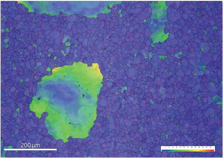
Figure 1a. Grain relative orientation distribution (GROD) map, showing numerous deformed grains (brighter colours) in a recrystallised matrix. Σ3 twin boundaries are marked by red lines.
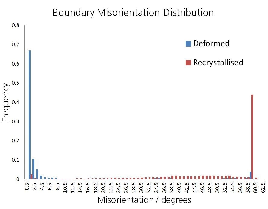
Figure 1b. Boundary misorientation frequency distribution, separated into the deformed grains and recrystallized grains.
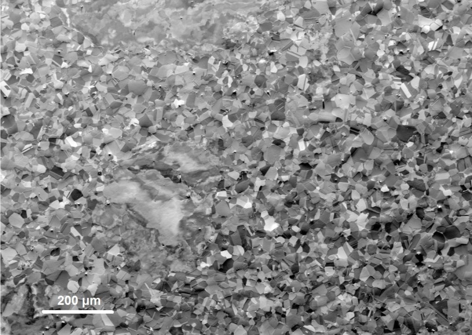
Figure 1c. Forescatter detector orientation image of the analysis area
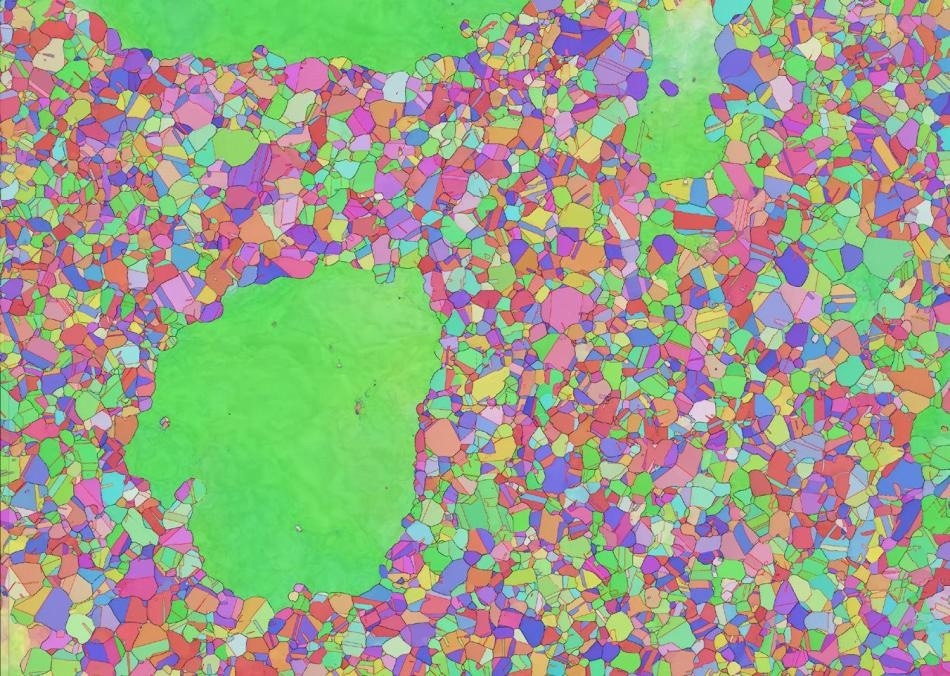
Figure 1d. Inverse pole figure orientation map showing grain boundaries in black and twin boundaries in red
Weld
In this example, Large Area Mapping was used to examine a welded sample of duplex stainless steel. The challenge was to analyze a wide transect (~ 5 mm across) yet to retain enough resolution to measure accurately the tiny grains in both the base metal and the weld itself. The area was mapped with a 0.25 µm step size, at ~ 2000 indexed patterns per second. A total of 96 maps were collected, totalling over 45 million points with a 98.5% hit rate. The resulting phase map (Figure 2a) clearly shows the difference from the base metal on the right to the fusion zone on the left. This large area, high resolution scan enables an in-depth analysis of the grain sizes, textures and phase distributions across the different zones of the weld.
In spite of the obvious change in the microstructure, there is no major change in the phase fraction between the base metal and the fusion zone (a ferrite to austenite ratio of 55:45 compared to 54:46 respectively). Yet, in the heat affected zone (HAZ), the phase fractions significantly change to 29% austenite and 71% ferrite.
Although the fusion zone seems to be considerably coarser grained, the full scale images shown in Figures 2b and 2c show the presence of many extremely small austenite grains measuring <5 µm in diameter. These reduce the mean grain size of the austenite in the fusion zone to just 6.3 µm, considerably less than the 9.5 µm mean in the base metal (both figures based on more than 20,000 grains).
The large area analysis also allows a statistically applicable study of the variation in texture across this weld margin. In Figures 2d and 2e, the contoured pole figures show the change in texture in the ferrite between the fusion zone and the base metal. Within the base metal, there is a relatively strong alignment of {100} poles normal to the rolling direction, but little clear texture is present in the fusion zone, with the higher densities arising from a few extremely large grains.
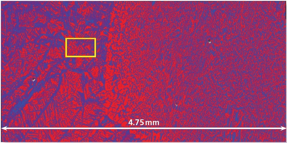
Figure 2a. Phase map across the weld margin in a duplex steel. Red – ferrite, blue – austenite. The fusion zone (weld) is to the left of the map, the base metal to the right. The yellow box marks the area highlighted.
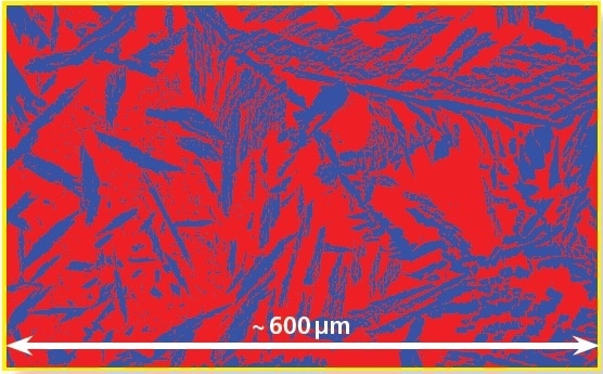
Figure 2b. Phase map of the area marked in (a) in higher detail. Red – ferrite, blue – austenite.
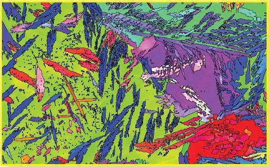
Figure 2c. Orientation map of the area marked in (a) in higher detail (inverse pole figure colour scheme, with grain boundaries in black).
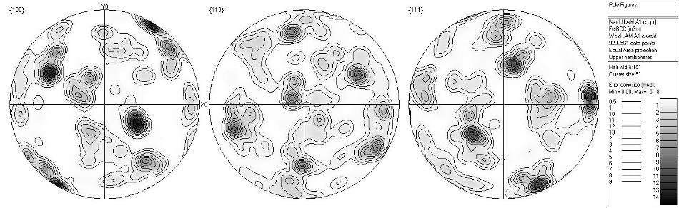
Figure 2d. Contoured pole figures ({100}, {110} and {111}) for ferrite within the fusion zone.
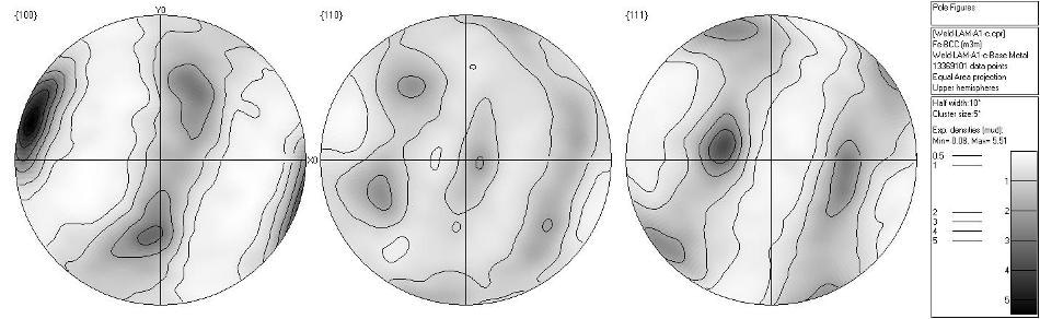
Figure 2e. Contoured pole figures ({100}, {110} and {111}) for ferrite within the base metal.
Conclusion
These two contrasting examples show how the combination of AZtec EBSD software and the Symmetry EBSD detector is an ideal combination for the effective and rapid characterization of a range of alloy and metal samples. In single phase metal samples, indexing speeds in excess of 3000 pps are obtained with no compromise on data quality or indexing hit rate, whereas more than 2000 pps are common in dual-phase materials. These speeds are attained without extraordinary beam currents: usually ~10 nA is sufficient to obtain exceptional pattern quality and indexing at 3000 pps.
With these high speeds and associated, uncompromised data quality, the Symmetry detector is shown to be an extremely powerful EBSD detector for texture, grain size and phase characterization of all but the most intricate samples. What took hours or even days with traditional CCD-based detectors can now be completed within a few minutes, expanding the appeal of EBSD as a routine characterization tool.

This information has been sourced, reviewed and adapted from materials provided by Oxford Instruments NanoAnalysis.
For more information on this source, please visit Oxford Instruments NanoAnalysis.