Electronic and computer processors with a higher speed need smaller features for integrated circuits (IC), which also need smoother and smaller substrate surfaces.
Chemical mechanical polishing (CMP) has emerged as one of the most important semiconductor fabrication technologies as it provides a more effective way of attaining adequate planarity for the production of the IC or hybrid bonding for advanced packaging and removing undesired topography in interlevel dielectric layers.
The CMP conditioner and the polishing conditioner pad strongly affect the planarization performance of the CMP technique. Due to this, a wealth of research has been undertaken in the selection and development of the CMP conditioner or pad, and the process of CMP conditioning as a whole.
This article outlines the analysis and measurement benefits that white light interferometry (WLI) provides for a range of CMP parts.
It additionally includes an improvement study that investigated the fluid layer’s asperity behavior beneath the wafer within the CMP process and showed the results of conditioning and polishing on the pads, along with wafer polish results.
Chemical Mechanical Polishing Technology
Also called planarization, CMP uses a combination of mechanical and chemical forces to smooth a wafer surface (see Figure 1).
The technique utilizes a corrosive and abrasive chemical slurry liquid along with a conditioning pad that is normally significantly bigger in diameter than that of the planarized wafer.
A dynamic polishing head is used to press the wafer and conditioner pad together, which is rotated with various axes of rotation with the slurry. The wafer is made flat (planar) because the process smooths any topography that is irregular and removes material. This procedure is usually required to prepare the wafer for the creation of more circuit components.
For instance, CMP can selectively remove material depending on its pad position or the complete surface can be brought within a photolithography system’s depth of field. For the most recent 5-nanometer technology roadmap, the standard depth of field requirements are down to angstrom levels.
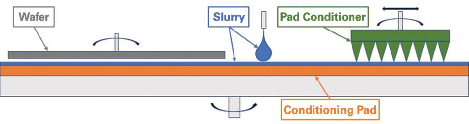
Figure 1. Typical functional principles of a CMP process. Image Credit: Bruker Nano Surfaces
An example of a popular innovation in CMP technology that demanded novel processes is when the semiconductor industry adopted copper conductors instead of aluminum conductors.
Various fabrication methods were utilized, including a range of techniques for patterning the metal and the use of metal barrier layers. Patterning metal is where the insulating layer underneath is patterned with open trenches where the conductor will be located.
The insulator is covered with a thick coating of copper that substantially overfills the trenches, and CMP is utilized to smooth the copper above the insulating layer.
The patterned conductor is created by the copper inside of the trenches of the insulating layer. A metal barrier layer must envelop all interconnections because the diffusion of copper into the nearby materials decreases their properties. A multilayer structure is produced with successive layers of copper and insulator.
This CMP technology would not be effective without the ability to stop repeatedly at the copper insulator interface and to remove the copper coating in an even manner.
Conditioning Pads and Pad Conditioners Use and Inspection
The surface features of the CMP conditioning pad are especially important as they influence the real area of wear, contact, friction, and lubrication in the polishing procedure. A urethane polymer is normally used to create the conditioner pad with numerous existing patterns that either modify the ability of the pad to hold the slurry or the surface rigidity.
WLI profilers from Bruker can stitch vast areas of the conditioning pads and can carry out automatic measurements, such as surface finish, depth, and width as an example.1
These analysis parameters are essential for the trench features to remove debris and retain slurry, and cannot be measured by the majority of other measurement devices (see Figure 2).
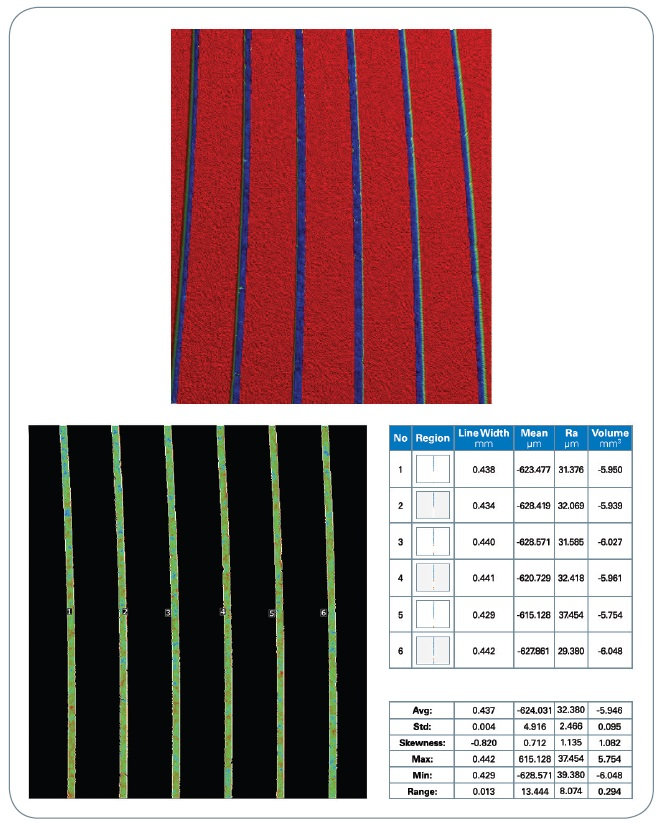
Figure 2. Conditioning pad automatic analysis. Image Credit: Bruker Nano Surfaces
A type of diamond-like carbide (DLC) or diamond grit coated pad conditioner is used to “condition” the surface of the conditioner pad itself. This is carried out both prior to and during the CMP procedure.
Most commonly a rotating pad conditioner disc is moved against the surface of the conditioning pad at a constant load. The pad conditioner’s structure slowly cuts the surface of the conditioning pad, shielding the surface from the accumulation of polishing debris, abrasive wear, plastic deformation, and various degrading elements.
This conditioning interaction enhances slurry transport, opens closed cells, and offers a consistent removal rate and polishing surface over time, restoring the valleys and peaks of the conditioning pad.
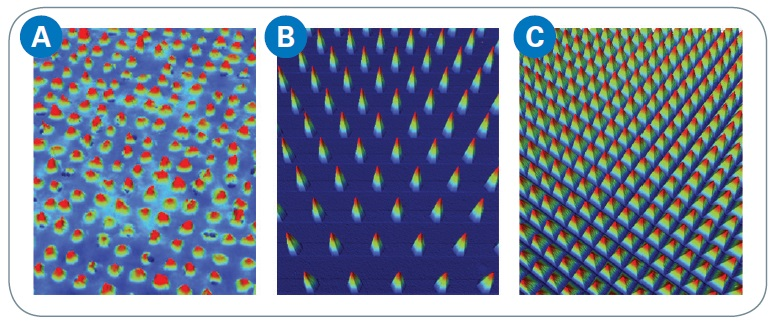
Figure 3. (a) Diamond pad versus two DLC-coated designed-structure pad conditioners (b and c). Image Credit: Bruker Nano Surfaces
At the same time, slurry abrasive particles slowly degrade the structures within the pad conditioner that interact with the surface of the conditioning pad. The initial interaction will arise on the tallest asperities of the surfaces when surfaces are brought together.
As the force on the surfaces increases, these asperities deform, and shorter asperities start to contact each other. The established relationship between reduced asperity height on the conditioner pad as a result of continued polishing and the consequent decrease in reliability and removal rate on the wafer is well documented.2
A relatively fast degradation of the removal rate is caused by a less than optimum conditioning process. When conditioning is too aggressive, the pad life decreases, and in time the conditioner pad itself will wear and damage the process of polishing.
Factors including crystal surface density, diamond crystal size, diamond crystal morphology and the DLC-coated designed construction (as outlined in Figure 3) have all been tested to create the optimum process of conditioning for the components being polished.
These structures can be automatically analyzed and detected by Bruker’s Vision64® software for diameter, volume, area, placement, density, pitch, height, and the total surface finish, as demonstrated in Figure 4 utilizing Vision64 Multiple Region analysis.
For these applications, WLI is the ideal measurement method because it can analyze these small areal structures that cannot be found using contact measurement systems. It also achieves the repeatability and nanometer vertical resolution necessary for this semiconductor industry application.
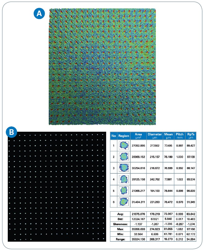
Figure 4. (a) 3D optical image of designed pad, and (b) automatic detection/analysis of the designed pad conditioner. Image Credit: Bruker Nano Surfaces
The Vision64 automatic Multiple Region analysis was carried out to measure the structures of the production pad conditioner and could easily locate, identify, and alert the user to structures that did not meet pre-determined tolerances for data logged parameters (view the graph in Figure 5).
The Peak % height in this example for each structure was entered onto the database with a pass/fail criteria that quickly identified debris, along with partially missing and chipped structures (for example, defects more than the red tolerance bands in Figure 6).
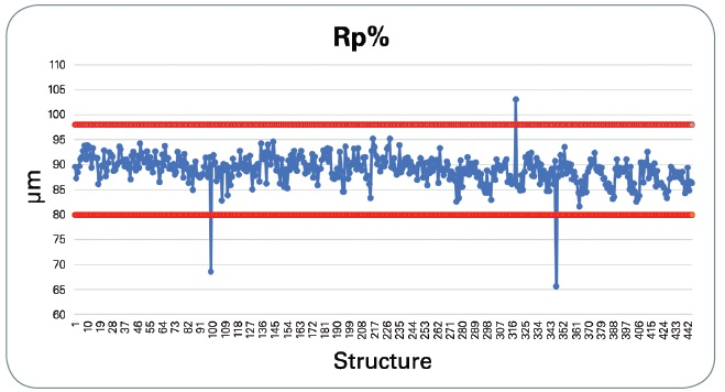
Figure 5. Individual peaks inspection of a pad conditioner logged to a database with Pass/Fail criteria. Image Credit: Bruker Nano Surfaces
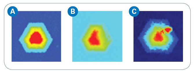
Figure 6. (a) Good structure, (b) missing peak causing LOW Rp%, and (c) debris causing HIGH Rp%. Image Credit: Bruker Nano Surfaces
As displayed in Figure 7a, the designed pad conditioner is usually spaced evenly around the perimeter of a bigger mounting platen. The WLI profiler from Bruker contains a self-calibrating laser that can carry out a thorough investigation on each of the five mounted pads. Those pads can be stitched together without taking any images from the in-between base platen itself, which saves a significant amount of time.3
This level of advanced remote analysis can verify that the pads are secured on the platen at the proper tilt angle, planarity, and location (see 7b-c). All of the WLI measurements can be exported into customer software for print evaluation and customized analysis.
A further benefit of the self-calibrating laser is that upon each measurement, the optical profiler self-calibrates which decreases the environmental and drift effects that are widespread when using other measurement devices. Found on high-end WLI systems, this feature provides the highest standard of repeatability and accuracy.
A Contact Coordinate Measurement Machine (CMM) cannot integrate the lateral resolution required for each separate pad because of the high aspect ratios and fine features. They also cannot perform remote pad location inspection.
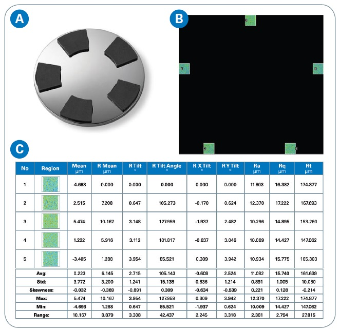
Figure 7. (a) Mounted Designed Pad structures, and (b and c) Automatic Analysis of Mounted Pad Conditioners. Image Credit: Bruker Nano Surfaces
In Bruker’s investigation, stitched WLI measurements were performed on a new pad conditioner. These measurements were contrasted against those of a used pad which was excluded from production as a result of insufficient CMP yield results.
When comparing the average mean height of the new and used mounted pads, the analysis showed that the pads were secured in line with the height specification because any mounting angle of those pads were averaged out (see Figure 8a).
Equivalent results would be achieved by a CMM or standard microscope. The WLI can additionally quantify the mounting angle of the individual pads, which clearly showed that Pad 3 was stitched at an extreme X-Y angle, generating the inadequate CMP results observed in the graphs in Figure 8b.
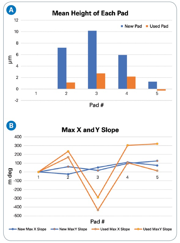
Figure 8. (a) Pad mean height versus (b) X–Y pad tilt angle of a new, good pad versus a used, bad pad. Image Credit: Bruker Nano Surfaces
CMP Wafer Polishing Results
The CMP process is constantly being developed, but it still has a few limitations, which means it can be one of the steps in certain semiconductor fabrication processes that creates the highest yield loss. A key issue is a continuous end-point detection, particularly with blind polishing, along with the physical damage to the wafer that can occur.
With this method, it is difficult to establish whether the intended amount of planarization has been achieved, or when the intended quantity of material has been removed, which could result in “hot spots” throughout wafer devices.
The CMP technique additionally should be observed to look at such uniformity displacement of dishing and damage to the devices itself, along with the isolation barriers. Bruker’s WLI optical profilers can be utilized to monitor this.
In these systems, the Vision64 software can subtract both stitched images and single images from wafer-to-wafer, or from inside of a wafer. A stitched image or reference image is taken which is then subtracted from consecutive measurements of homogeneous areas.
The subtraction element can apply filtering as required to the pre- and post-subtraction image(s), align images run to run, and exclude pre-image waviness and form. This is highly beneficial when tracking height deviations from the CMP lapping steps or growing the wafer (see Figure 9).
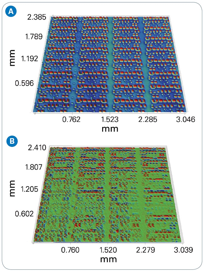
Figure 9. (a) Z-scaled ±70 nm reference image, and (b) Z-scaled ±0.8 nm subtracted image. Image Credit: Bruker Nano Surfaces
Die flatness is necessary for wafer-to-die or die-to-die bonding, or with chiplets (dielets) in various packaging to confirm sufficient molecular-level adhesion between facing surfaces. Voids, along with possible interconnection issues can be a result of nanometer height differences in peaks or valleys.
The lateral micrometric resolution is necessary to enable the sufficient recording of structures like T-Box and via openings. The WLI method is the only one that can meet all the criteria with its fusion of angstrom vertical resolution and the ability to maintain micrometric lateral resolution over vast, stitched regions of hundreds of millimeters squared (shown in Figure 10).
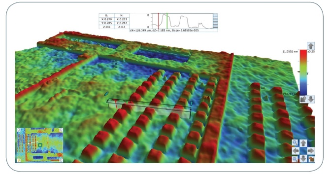
Figure 10. 4.6 x 2.5 mm field of view of a CMP-processed wafer with nanometer structures and T-Box openings. Image Credit: Bruker Nano Surfaces
Research Case Study: CMP Polishing for Characterizing and Evaluating Pad Conditioners
Bruker application engineers collaborated with a pad conditioner manufacturer, a conditioning pad manufacturer, a major CMP equipment manufacturer, a semiconductor wafer manufacturer, and academic researchers to carry out a series of investigations to research diamond conditioner wear on a CMP device by contrasting WLI images taken prior to and after extended controlled wear testing.
A WLI profiler from Bruker was utilized to analyze feature surface heights, pad roughness, planarity, and bow from 0.1 nanometer to many millimeters. Using a range of 3D and 2D evaluation of the WLI interferometric data, the recognized peaks of particular, known diamond structures were contrasted before and after wear testing.
High lateral resolution (~3.24 microns) was achieved as the imaged regions were moderately large with up to 4.3 x 6.5 millimeters across stitched scans. After wear testing, shifts in these peaks that were identified enabled the measurement of wear on the conditioning pad.
Figure 11 outlines a three-dimensional analysis before and after wear testing of the same diamond group. This technique was then utilized to analyze unique conditioner designs for longer lasting and more efficient CMP pad conditioning.
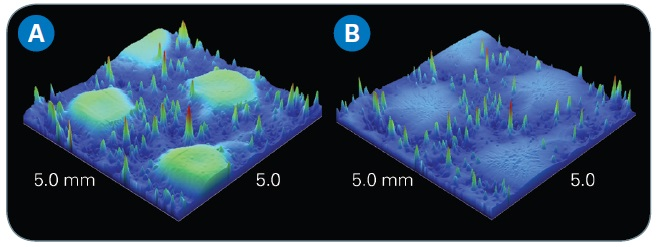
Figure 11. (a) Diamond before testing, and (b) the same diamond after the wear test. Image Credit: Bruker Nano Surfaces
A conditioning tool was utilized to measure diamond wear before and after extended wear testing through the numerical matching of interferometry images recorded in overlapping areas.
The biggest common region shared by two images was identified by a matching algorithm, and the final image was reoriented to yield the optimum match with the first image in the binding metallization.
Usable results were reliant on the presence of an area inside of the pad conditioner, segments of the binding metallization, that was in the interferometer’s focal range and was far enough from the surface of the polishing pad to have insignificant wear.
By utilizing surface height probability density functions to characterize the images, peaks in the height distributions were located that correlated with groups of diamonds or single diamonds.
An estimate of the mean wear rate was determined by the shifts in the peaks after wear testing. The wear rate was very low, with an average of 5 x 10⁻⁴ microns each minute across 710 minutes. The WLI profiler’s large sample area and high resolution allowed the wear at this level to be detected.
Diamonds on the outside edge of the device wore faster than ones in the center, and the higher diamonds were generally found to wear more efficiently than the shorter ones. This microwear was additionally found to correspond with a steady decline in pad cut rate.
Throughout the lifecycle of the pad conditioner, every diamond that creates a furrow on the pad surface should provide both plowing, where the material is pushed aside, and cutting, where material is excluded from the furrow.
It was suggested that the decline in cut rate correlated to an increase in the amount of pad material that was plowed instead of being cut while the sharp points and edges on the contacting diamonds broke down.
The researchers summarized from this data that the decrease in cut rate with conditioner age was the result of an increase in plowing and a decrease in cutting as contacting diamond tips and edges break down.
Further research using the majority of the factors outlined above were able to measure extended wear for innovative diamond pad conditioner designs, with the goal of engineering a pad conditioner that would resist abrasive wear and corrosion more effectively while maintaining sufficient CMP pad polish.
A Bruker WLI optical profiler was utilized by researchers to analyze the surface of the diamond conditioner, both before and after the 30-hour conditioner wear and polishing procedure.
A template was employed to choose the regions for analysis which ensured that the same regions were imaged before and after the extended wear test. A polytetrafluorethylene film was used to coat the experimental designs to decrease chemical attack and substrate wear.
The pad conditioner was mounted on a different polishing tool for in-situ polishing of copper wafers at intervals during the wear experiments. Real-time copper removal, shear force, and pad temperature rates were quantified.
WLI was carried out on chosen regions of the conditioner surfaces before and after wear testing to measure differences. Interferometry analysis showed that plastic deformation and shear forces laterally displaced the coating material from the diamond-free zones and resulted in the adjacent diamonds being partially or totally covered.
Contours around multiple diamonds analyzed at the same level were also found to tighten on the used conditioner. This suggests that the coating instantly surrounded some of the diamonds that had been displaced and that those diamonds were active.
Using these results and synchronous data from thermal observation methods and WLI, the investigators were able to demonstrate that the coating on the pad conditioners offered protection from abrasive and chemical damage, showing that even after 30 hours, performance did not decline.
One of the designs was also shown to offer a tool for gradually exposing more diamonds to the pad as they wear.
Conclusions
WLI profilers from Bruker have the novel capability to execute three-dimensional, efficient, high-resolution, contactless surface texture mapping at sub-nanometer height scales.
This makes these systems the superior metrology technique for the characterization of pad conditioners, conditioner pads, and other elements within the CMP process, such as wafer inspection. The conditioner pads automatically identify manufacturing defects while being inspected for trench depth and width.
Pad conditioners can be analyzed for diamond density, surface finish, structure defect inspection, peak uniformity, and total pad bonding to the platen.
The resulting CMP processed devices can additionally be audited for CMP hotspots and planarity, surface finish, over (dishing/erosion) and under polishing, depths, heights, and widths, and much more.
3D optical profilers from Bruker offer a way of measuring various elements of the CMP process and will prove to be invaluable in the pursuit of more efficient processing and increasingly small semiconductor features, along with superior wafer-/die-level bonding for advanced packaging.
Acknowledgments
Produced from materials originally authored by Roger Posusta and Samuel Lesko from Bruker.
References and Further Reading
- Want, JC, Computerized interferometric measurement of surface microstructure, Proc. SPIE 2576, pp. 26-37 (1995).
- Novak E, White-light Optical Profiler with Integrated Primary Standard, XVII IMEKO World Congress (2003).
- Gray, CD et al., “Viewing Asperity Behavior Under the Wafer during CMP,” Electrochem. and Solid-State Ltrs., Vol. 8, No. 5, pp. 1–3 (2005).
- Stein, D. et al., “Optical Interferometry for Surface Measurements of CMP Pads,” Journal of Electronic Materials, Vol. 25, No. 10, pp. 1623–27 (1996).
- Dyer, T., and J. Schlueter, “Characterizing CMP Pad Conditioning Using Diamond Abrasives,” Micro, Vol. 20, pp. 47–54 (2002).
- Oliver, MR, et al., “CMP Pad Surface Roughness and CMP Removal Rate,” Chemical Mechanical Planarization IV, Vol. 2000–26, pp. 77–83 (2001).
- Kincal, S., “Impact of Polish Pad Imperfections on Chemical Mechanical Polishing Defects,” J. Electrochem. Soc., Vol. 153, No. 8, pp. G742–G745 (2006).
- Borucki, L., et al., “Measurement of Diamond Conditioner Microwear,” Proc. of 22nd VLSI Multilevel Interconnection Conference (VMIC), pp. 441–45 (2005).
- Borucki, L., et al., “Diamond Conditioner Wear Characterization for a Copper CMP Process,” Proc. of PacRim—CMP 2005 the 2nd International Conference on Planarization CMP and its Application Technology, pp. 147–52 (2005).

This information has been sourced, reviewed and adapted from materials provided by Bruker Nano Surfaces.
For more information on this source, please visit Bruker Nano Surfaces.