InSight 300 is a fabrication-ready, automated atomic force microscope (AAFM) engineered for dependable and economical inline metrology in high-volume semiconductor production settings. Boasting a scanner flatness of less than ±1 nanometer and a best-in-class noise level below 35 pm, this system satisfies the demanding needs of advanced Chemical Mechanical Planarization (CMP) and etch processes, spanning from micron-scale roughness measurements to fully automated defect inspection of bare wafers.
Its profilometry features meet and surpass the millimeter-scale and bevel-edge metrology requirements for state-of-the-art hybrid bonding applications. Furthermore, the InSight 300 incorporates Bruker's unique operating modes for optimized measurements of sidewall roughness, automated bare-wafer defect review, and sophisticated profiling of feature surfaces.
Best-in-Class Accuracy and Stability
The system features a high-performance tip scanner integrated with Bruker's ultra-flat profilometer stage, enabling nanometer-level precision.
<5 Minutes Recipe Creation
Dedicated application modes simplify operation, guaranteeing accurate metrology data for any user at any time.
Trusted Reliability
Bruker's 25 years of focused expertise in fabrication technology ensure the optimal solution for high-volume manufacturing (HVM) environments.
Features
High-Throughput AFM for Accurate Inline Measurements
The InSight 300 benefits from Bruker's 25 years of AFM innovation, resulting in enhanced resolution, stability, versatility, and user-friendliness. Its outstanding throughput, accuracy, and reliability guarantee dependable results while maintaining a low overall cost of ownership.
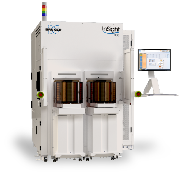
Image Credit: Bruker Nano Surfaces and Metrology
InSight 300 Features:
- Modern GUI
- Specialized Probes
- Versatile Optics
- Application-Specific Modes
- Continuous Performance Verification
- Automatic Tip Management
Built with Semiconductor Metrology Expertise
Experience, Service, and Support
Bruker automated atomic force microscopes (AAFMs) have a long-standing reputation as a reliable solution for semiconductor fabrication facilities globally. From the initial fully automated 200 mm fab AFM to the current InSight 300, Bruker has pioneered patented AAFM innovations that have facilitated the ongoing advancement of next-generation semiconductor devices.
Bruker is committed to ensuring the equipment operates at maximum uptime and productivity. Bruker provides:
- A global service and support team renowned for resolving issues effectively on the first attempt.
- Strategically located service depots ensure readily available parts.
- A range of service coverage plans tailored to the unique support needs.
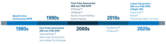
Bruker's semiconductor metrology innovation timeline. Image Credit: Bruker Nano Surfaces and Metrology
Specialized Probes
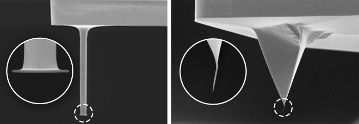
(left) CDR1000-10UM probe for sidewall imaging. (right) BNT-500-12 probe with a >500 nm long EBD spike, suitable for a multitude of applications. Image Credit: Bruker Nano Surfaces and Metrology
Application-specific probes ensure the most dependable and precise characterization of advanced technology nodes. Bruker is the only AFM manufacturer that also owns and operates a dedicated probe nanofabrication facility, allowing it to continuously develop innovative probe designs optimized for particular applications.
Focused on Production
Superior Capabilities
The InSight 300 provides stable, NIST-traceable, and artifact-free data. Its integrated intelligence enables accurate and repeatable:
- Hybrid bonding
- Roughness metrology
- Automatic defect review
- Depth metrology
- Sidewall profiling
- Surface profiling
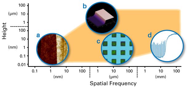
Map representing field of view, spatial frequencies and height ranges covered by Insight 300’s AFM and profiling capabilities. Examples shown are (a) atomic steps on 2D material, (b) 10 µm step height, (c) 100 µm bond pad metrology scan, and (d) >20 mm profile scan. Image Credit: Bruker Nano Surfaces and Metrology
Application-Specific Modes
Application-specific operating modes ensure maximum metrology accuracy while optimizing throughput. The InSight 300 features Bruker's patented operating modes precisely engineered for roughness measurements (TrueSense®), sidewall roughness and angle determination (CDMode), depth measurement of high aspect ratio structures (DTMode), and surface profiling.
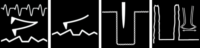
Bruker’s specialized application-dedicated operating modes: TrueSense®, Profiling, DTMode, and CDMode. Image Credit: Bruker Nano Surfaces and Metrology
Automatic Tip Management
The TipX technology on the InSight 300 offers genuine probe automation and complete quality assurance for high-volume manufacturing. Probes are automatically loaded and qualified to ensure they meet all recipe specifications. The reliable vacuum probe holding mechanism provides maximum flexibility in probe selection and lowers probe costs.
(left) Automatic probe shape qualification. (right) Probe cassette with a 25-probe capacity. Image Credit: Bruker Nano Surfaces and Metrology
Verified Performance
The development and production processes include continuous verification and confirmation of performance through extensive long-term stability, linearity, and accuracy testing. With less than ±1 nanometer of out-of-plane motion across the entire 105 µm2 scan area and a Z-range of up to 18 µm, combined with a long-range profiling stage, the InSight 300’s AFM scanner, featuring a scanning-tip design, is optimized to address contemporary nanoscale metrology challenges.
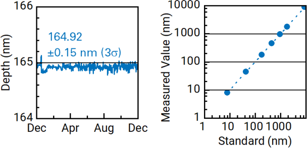
(left) Statistical process control chart showing sub-nanometer long-term stability. (right) Step height on VLSI reference samples showing high accuracy and linearity. Image Credit: Bruker Nano Surfaces and Metrology
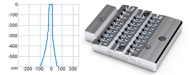
Versatile Optics
The InSight 300's integrated optics facilitate easy navigation to regions of interest and the efficient creation of recipe sites. A combined dual-channel, tip-centric objective and a third offset objective deliver unparalleled optical resolution while preserving maximum field of view (FOV).
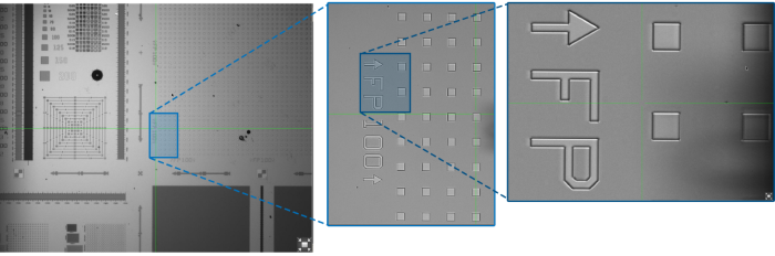
The field of view and resolution for InSight 300’s integrated optics is illustrated on a MetroBoost FP100 reference structure. Image Credit: Bruker Nano Surfaces and Metrology
Modern GUI
The InSight 300 is designed for user-friendliness. An intuitive graphical user interface (GUI) allows technicians and engineers to quickly create effective recipes, including recipe-driven tip management and resource tracking. Recipes can be developed and modified offline, ensuring the tool remains in production during development cycles.
Automated wafer map generation and recipe wizard. Image Credit: Bruker Nano Surfaces and Metrology
Applications
Optimized for Applications
Roughness Metrology
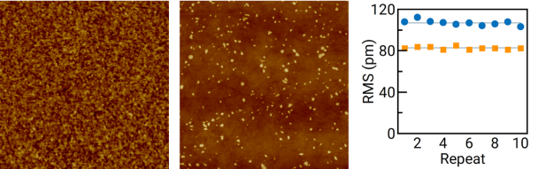
(left) Ultrasmooth Si (85 pm RMS, 1 nm Z scale, 1 × 1 µm scan). (middle) Post-CMP ILD area with 0.42 nm RMS (8 nm Z scale, 3 × 3 µm scan). (right) High-throughput roughness metrology repeatability result on two Si wafers with 106 pm RMS and 83 pm RMS, 3 σ<5 pm. Acquired at <1 min MAM time. Image Credit: Bruker Nano Surfaces and Metrology
The InSight 300's industry-leading low noise levels allow for sub-angstrom surface roughness control, providing quantitative roughness measurements below 100 pm RMS. Even with short Measurement-Analysis-Move (MAM) times of approximately one minute per site, roughness data remains accurate and dependable, exhibiting excellent repeatability (e.g., 3 sigma <10 pm for smooth surfaces with RMS roughness <1 nanometer) and consistent results across different tips.
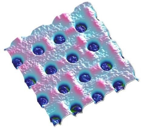
Depth Metrology
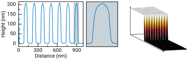
(left) DTMode scan and (right) section profiles of a dense array of vias (depths 80 to 100 nm), enabling within-wafer process variation studies. Image Credit: Bruker Nano Surfaces and Metrology
Bruker's proprietary Deep Trench mode (DTMode) is specifically designed for characterizing narrow trenches and vias with depths ranging from tens of nanometers to over 10 µm. Achieving a Measurement-Analysis-Move (MAM) time of less than 10 seconds, DTMode, when used with application-specific high aspect ratio tips, fulfills the depth metrology requirements for high-volume manufacturing (HVM) etch process control.
Sidewall Profiling
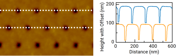
(left) CDMode characterizes a line/space pattern with 150 nm pitch for (middle) high-resolution SWA, and (right) line edge roughness. Image Credit: Bruker Nano Surfaces and Metrology
Sidewall angle (SWA) and sidewall roughness (SWR) are crucial parameters for device and integrated circuit (IC) performance. Accurate measurement of these critical dimensions using AFM necessitates a mode specifically designed for this metrology; simply tilting a scanner introduces significant Total Measurement Uncertainty (TMU). Bruker's critical dimension scan mode (CDMode) is the world's only genuine CD-AFM metrology technique, offering unparalleled accuracy, unmatched repeatability, and the industry's lowest proven TMU.
Automatic Defect Review
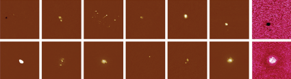
High-resolution height scans of various nanometer-scale defects (2x2 µm scans), and simultaneously acquired adhesion measurements (final two images, in pink) further aiding defect classification. Image Credit: Bruker Nano Surfaces and Metrology
Sidewall angle (SWA) and sidewall roughness (SWR) are crucial parameters for device and integrated circuits.
AFM defect review offers a non-destructive alternative to conventional review methods like SEM/EDX, and uniquely provides adhesion measurements, further assisting in defect classification. The InSight 300's defect review process can be fully automated and driven by recipes, with KLARF compatibility. Maximum productivity is achieved through quick recipe creation in under five minutes and automated bare wafer registration, enabling throughputs of tens of defects per hour.
Surface Profiling
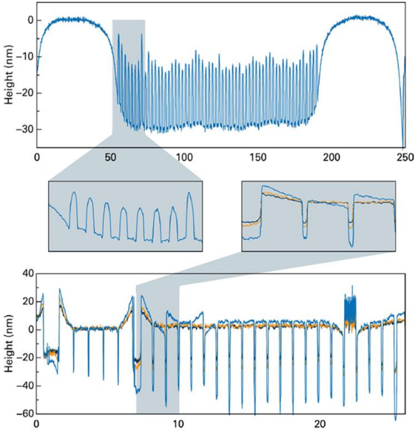
Post-CMP profiling (2 nm data spacing) with high repeatability for both dishing (3σ = 0.14 nm) and erosion metrology (3σ = 0.32 nm). Image Credit: Bruker Nano Surfaces and Metrology
The InSight 300 can be equipped with leading-edge profiling capabilities. Measurements can span distances up to 50 millimeters at speeds reaching 1 millimeter per second, facilitated by advanced non-contact linear stage motion optimized for both local and long-range flatness. Profiling applications include post-CMP characterization of dishing and erosion, bevel edge rounding analysis, and step height measurements.
Hybrid Bonding
Cu/ILD pattern post-CMP revealing critical roughness and recess depth information for the hybrid bonding process. Image Credit: Bruker Nano Surfaces and Metrology
The InSight 300 automated AFM applies to the latest hybrid bonding technology nodes, offering high-resolution imaging and specialized analysis for critical bond pad metrology and automated bevel edge metrology for hybrid bonding processes.
Specifications
InSight 300 Automation Specifications
Each wafer manufacturing facility and semiconductor fab presents unique requirements and challenges. The product specifications and offerings are a foundation for tailored discussions with experts to assess how available capabilities can best address specific needs.
Source: Bruker Nano Surfaces and Metrology
| |
|
| Fab Automation |
SECS/GEM Host Automation Interface, E84 PI/O AMHS support |
| SEMI Standards E4, E5, E30, E37 & E37.1, E39 & E39.1, E40, E87 & E87.1, E90, E94, E116 & E116.1 |
| Regulatory Compliance: CE, UKCA, KC, SEMI S2/S8, F47, 21 CFR 1040.10, 21 CFR 1020.40 |
| Tip Handling |
Automated Tip Management and Tip Exchange |
| Tip Capacity: 4 Cassettes, 25 Tips each |