Discover everything there is to know about reverse tip sample scanning probe microscopy (RTS SPM) and its main applications.
In your opinion, what is the primary limitation of SPM, and how is the field working to overcome it?
Nemanja Peric:
The biggest challenge with SPM is that the SPM data quality is inherently linked to the tip quality. As we all know, since its inception, SPM has become one of the go-to methods for nanoscale characterization because of atomic resolution capability and versatility, which stems from the fact that the technique can be used to measure all kinds of material properties. But the core issue is that the working principle is based on probing tip-sample interactions, and thus the tip quality is a crucial factor.
If your tip is sharp and clean, you’ll get great data. But all tips eventually degrade during the measurements. They wear down, get contaminated, or just lose sharpness and that will directly impact your results. So, when that happens, a simple fix is just to swap out the tip. The problem is that this is often a manual process, which takes time, and interrupts your measurement workflow.
A lot of the innovation in the field right now is focused on overcoming this limitation. People are working on ways to automate the tip replacement process or at least, make it faster and more reliable. This will not only improve the throughput but also make SPM results more trustworthy.
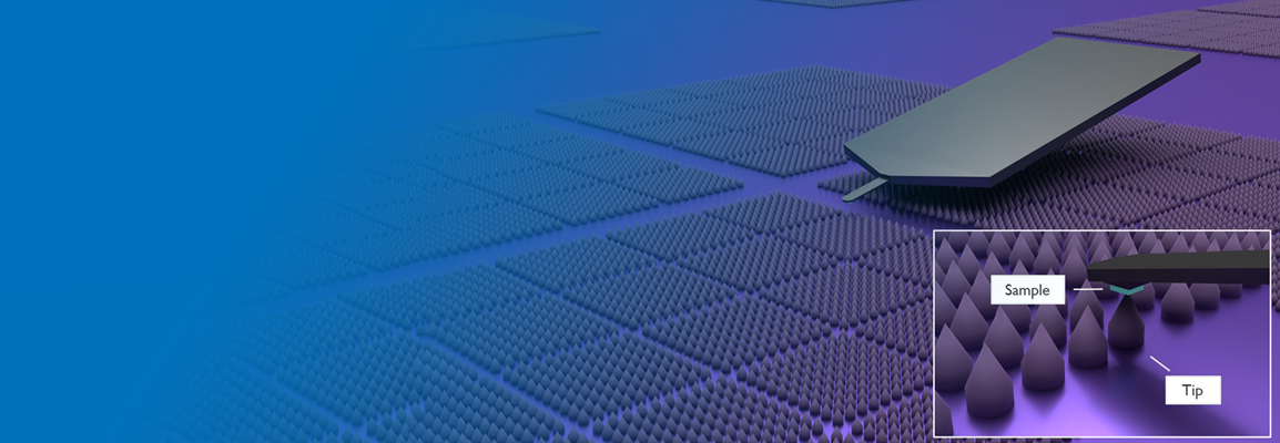
Image Credit: Bruker
On that note, what exactly is RTS SPM concept, and how does it address these tip-related challenges? What sets it apart from conventional SPM?
Nemanja Peric:
RTS SPM stands for Reverse Tip Sample Scanning Probe Microscopy. It’s a new concept that shifts the paradigm from scanning the sample to scanning the tip instead, by simply reversing the positions of the tip and the sample.
In RTS SPM, instead of having just one tip on a cantilever and the sample right below, the RTS configuration makes use of a nanofabricated RTS probe chip that hosts thousands of identical sharp tips arranged in a dense array. This chip is then placed where you'd normally put the sample, while the actual sample is mounted on a tipless cantilever.
What’s really powerful about this setup is that it makes the tip exchange almost instant. If a tip wears out and you need a new one, you just need to reposition the cantilever holding the sample to the next fresh tip using either piezo or course movement, which takes only seconds to complete. Compare that to conventional SPM, where changing a worn tip can take anywhere from 10 minutes in air to several hours in high vacuum, involving tedious manual replacement, realignment, re-engagement with the sample surface, and again finding the region of interest.
So, with the RTS configuration, tip exchange is not only faster and simpler, but it also happens without disrupting the ongoing experiment. Additionally, the RTS concept doesn’t require any hardware modifications to existing commercial AFM systems and it’s fully compatible with all the operational modes and working environments because it doesn’t change the underlying physics, it just flips things around. That makes it especially appealing for applications where frequent tip changes are needed.
What is the process for fabricating RTS probe chips, and how are they designed for optimal performance?
Pieter Lagrain:
The RTS concept fundamentally depends on having an RTS probe chip, so naturally, this was indeed the starting point for us. We ended up developing a new fabrication protocol based on dry etching. The main goals were to keep the process simple, reproducible, cost-effective and time efficient enough to be completed in short time.
We published the fabrication process in 2024 in the Nanotechnology journal (DOI 10.1088/1361-6528/ad3744); a paper that also served as the first detailed introduction of the RTS concept. You can find all the technical details there, but I will give here a quick overview.
It starts with designing a mask that defines the layout of the tips on the RTS probe chip. We chose a 25 μm spacing between the tips, which allows us to access up to nine different tips using only the piezo movement. The fabrication process begins with patterning that mask on a standard <100> silicon wafer. We spin-coat the wafer with a photoresist, then use UV lithography to transfer the pattern. After that, we go through a series of ICP-RIE tip etching steps, along with plasma cleaning and sharpening steps, which results in an array of sharp, nearly identical silicon tips. In the same work, we’ve also demonstrated how the RTS concept can be extended to suit different applications, by coating these silicon probe chips with boron-doped diamond for high-force ones, and with platinum for electrical SPM measurements.
So, while we’ve developed what we believe are optimal RTS probe chip designs for our specific use cases, what’s important is that the fabrication process is flexible so that it can be adapted to other needs.
Having the RTS probe chips is one part but how do you actually handle the samples? Specifically, how do you mount samples onto a tipless cantilever for RTS SPM?
Pieter Lagrain:
The probe chip is essential to make RTS work, but the other half of the equation is indeed the sample preparation, and that part can be more tricky. There are a few factors to be considered, like the size and shape of the sample, the stiffness of the cantilever, and most importantly, the method you use to attach the sample.
You really need to choose carefully or sometimes even invent a new method that fits your specific application. In our work, we’ve explored several techniques, including direct material deposition, seeding, and various forms of sample transfer with great success. But the one I’d like to emphasize here is the method based on focused ion beam (FIB) technology because it is well established and much used in the nanoelectronics domain.
Following our original RTS SPM paper, we published shortly afterwards another article (DOI 10.1016/j.mne.2024.100247) focused entirely on sample preparation using a dual-beam FIB/SEM system. This paper describes the first complete workflows for mounting both top-view and cross-sectional samples onto tipless cantilevers reliably and with good time efficiency. Less than 90 minutes per sample, in fact. We actually drew on our experience with preparing TEM samples to develop these procedures.
But, of course, this is still an area with a lot of room for innovation. As RTS SPM further evolves, I expect that new, even more efficient sample prep methods will emerge especially when more people start working with the technique.
What kinds of measurements have you done using the RTS configuration, and how do they compare to what you would get with a conventional SPM setup?
Nemanja Peric:
We’ve done a range of different measurements using the RTS configuration, but maybe the best place to start with is a simple basic topography measurement, since it is a good benchmark to directly compare RTS with conventional SPM.
The nice thing about the RTS concept is that it doesn’t change the process of how you perform the measurements. You just engage the sample with any one of the thousands of available tips on the RTS probe chip and start scanning in the same way as you would do in a regular setup.
To give you an example, in the RTS configuration, we scanned the exact same diamond nanoparticle using nine different tips on the same silicon RTS probe chip. This gave us nine slightly different perspectives, and we could clearly see which tip gave us the sharpest, most detailed image. That kind of comparative analysis is technically possible with conventional SPM, but it would be quite time-consuming, expensive and thus, impractical. While in RTS SPM it is straightforward. So even in something as routine as topography measurements, the RTS concept can add value by bringing extra statistical robustness to your data.
And moving beyond simple topography, have you explored more advanced SPM modes using the RTS configuration?
Nemanja Peric:
Yes, in fact, the value of seamless tip switching becomes even more apparent when you go beyond basic topography into more advanced modes. We’ve explored other RTS applications with our platinum and boron-doped diamond functionalized silicon probe chips.
Specifically, we’ve successfully performed CAFM, KPFM, and SSRM across a range of sample types. And in every case, the measurements we got were on par with what you'd expect from a conventional SPM setup. The key difference was again the ability to quickly and easily switch to a fresh tip without interrupting the measurement workflow.
Take SSRM, for example. It’s a high-force SPM mode widely used in both research and the semiconductor industry to quantitatively map carrier concentration profiles in nanoelectronic devices. It’s a powerful method, but rapid tip wear is a major drawback. Even though SSRM tips are diamond-based, they degrade quickly at the required giga-pascal pressure, which means you’re constantly needing to replace them. With RTS SSRM, we’ve shown that you can just shift to a fresh tip in seconds and keep going. That drastically improves throughput and lets you build up a large, statistically meaningful dataset.
What do you see as the future of RTS SPM? How do you think the technology will evolve, and what challenges still remain?
Nemanja Peric:
I’d say most people in the SPM community would agree that having easy access to what is essentially an unlimited number of tips, without the hassle of manual replacement, is something we've always wished for. RTS SPM now offers that as a real, practical solution, so I think the potential of RTS SPM is pretty clear.
That said, we’re still in the very early days of this technology. There’s a lot of room for growth, both in terms of new applications and in optimization. For example, RTS SPM could be a great fit for areas where scaling certain SPM measurements to match industrial throughput has been a challenge. On the technical side, I think we’ll see a continued development in sample preparation methodologies, making it easier, faster, and more flexible to mount different types of samples onto tipless cantilevers. Another area is the design and fabrication of new RTS probe chip types tailored to specific applications. That could really broaden the range of what RTS SPM can do.
And, in fact, what the RTS concept will ultimately be used for in practice will largely depend on the SPM community and on different groups picking it up, adapting it, and exploring how it could benefit their own work. In the end, RTS SPM is just an alternative way of doing SPM, but the one that could open the door for many new possibilities.
Watch the full webinar
About the Speakers

Nemanja Peric received his PhD degree from the University of Lille (France) while working at the Institut d’électronique de microélectronique et de nanotechnologie (IEMN/CNRS). After a short postdoctoral research period at IEMN, Nemanja joined imec in Leuven (Belgium) where he is currently working as an SPM researcher. His interests and expertise involve mainly AFM and STM.

Pieter Lagrain received a master degree in chemical engineering from KU Leuven (Belgium). He joined afterwards imec as an engineer for nanoelectronics device analysis. His interest and expertise mainly involve FIB, TEM and SPM.

This information has been sourced, reviewed, and adapted from materials provided by Bruker Nano Surfaces and Metrology.
For more information on this source, please visit Bruker Nano Surfaces and Metrology.
Disclaimer: The views expressed here are those of the interviewee and do not necessarily represent the views of AZoM.com Limited (T/A) AZoNetwork, the owner and operator of this website. This disclaimer forms part of the Terms and Conditions of use of this website.