Dielectric materials are vitally important in the function of microelectronic devices, as these materials electrically isolate conductive components from each other in microcircuits.
Capacitance between conductors has the potential to limit a circuit’s maximum operating frequency, and capacitance increases in inverse proportion to the separation distance between conductors. To minimize a microelectronic device’s size whilst maximizing its operating frequency, a device’s components should be separated by a material possessing a dielectric constant that is as low as possible.
A class of materials referred to as ultra low-k (ULK) dielectrics are commonly used for this task. All significant semiconductor node changes necessitate the effective integration of a new generation of lower k materials with higher porosity. There is a considerable trade-off, however, between electrical properties and mechanical properties for low-k materials.
Incorporating nanometer-scale pores to decrease k generally results in reduced strength, adhesion and stiffness of the deposited films. Monitoring the mechanical properties of ULK films throughout a semiconductor production process is therefore essential if the device is to survive while yielding a reliable, consistent finished product.
This article explores how monitoring the mechanical reliability of ULK films has become progressively more important in rapidly identifying process variation while sustaining high device yields. It also outlines how nanoindentation and nanoscratch testing can offer an ideal means of measuring these critical films’ modulus (stiffness), hardness (strength), and critical scratch force (adhesion).
Nanoindentation Testing
The nanoindentation testing of ULK films is achieved by forcing a diamond pyramidal probe into the film according to a specified force, holding this force for a number of seconds, and then eventually withdrawing the probe. Both force and displacement are continuously measured during the test, giving researchers a basis by which the material’s modulus and hardness can then be calculated.1
Figure 1 displays a force-displacement curve acquired during a test on a 200 nm thick ULK film. A cube-corner geometry was utilized due to acute geometry, allowing it to penetrate through a thin, comparatively dense skin layer on the surface of the ULK film, effectively probing the film’s interior properties.
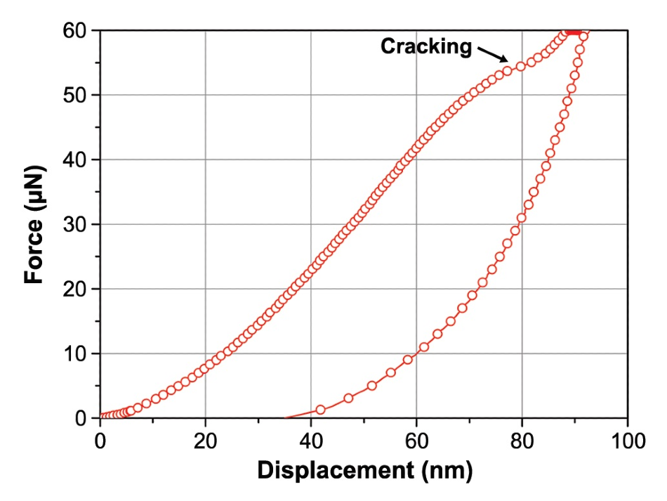
Figure 1. Representative force-displacement curve from an indent on a ULK film. Image Credit: Bruker Nano Surfaces
However, should the indent be too deep, the measurement will be affected by the silicon substrate’s properties. The most accurate measurement of the film’s properties tends to be obtained when the indent depth is slightly beyond the depth required to penetrate the surface layer.2
Nanoindentation, because of its small scale, enables highly localized characterization of the mechanical properties of a material. Furthermore, when nanoindentation tests are conducted in arrays, it can also be used to generate maps of the mechanical properties of larger surface areas.
Bruker's Nanomechanical Metrology Tool (NMT) series of instruments has been specifically designed for nanomechanical testing as part of process control applications. The translation stage of the ATI 8800 (shown in Figure 2) can accommodate silicon wafers up to 300 mm diameter, providing adequate range to reach any area on the wafer.
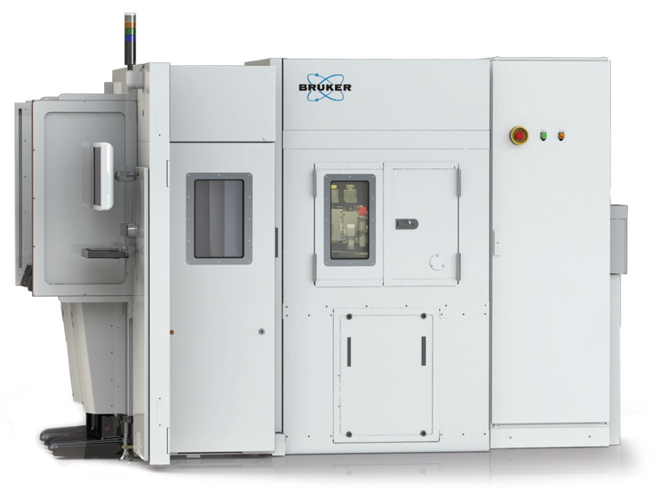
Figure 2. Bruker's ATI 8800, fully automated nanomechanical metrology tool for 24/7 wafer process monitoring. Image Credit: Bruker Nano Surfaces
The ATI 8800 can also be utilized to conduct a series of tests in a pre-determined area of a wafer, allowing users to check for inter-wafer process variability or to map mechanical properties over a specific area.
In this instance, a series of 1,884 nanoindentation tests were conducted to ascertain the homogeneity of a ULK film’s mechanical properties across the whole surface of a 300 mm wafer (see Figure 3). The mechanical property maps generated via this array of tests uncovered variations in hardness and modulus of between ~10 and 15% across the ULK film’s surface.
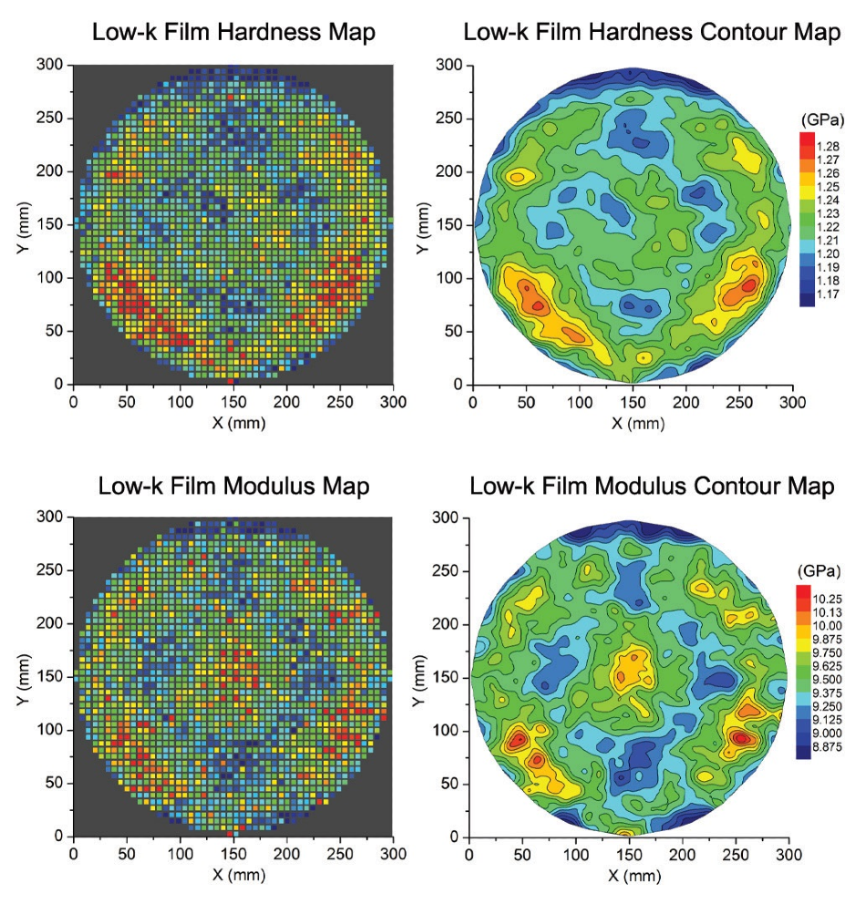
Figure 3. Results from 1,884 nanoindentation tests on a 200 nm ULK film, showing a property variability of 10 to 15% due to non-uniform processing conditions. Image Credit: Bruker Nano Surfaces
Nanoscratch Testing
Nanoscratch tests were conducted in order to measure the adhesion of the ULK film to the underlying substrate. Each individual scratch test was performed by moving the probe laterally (in the plane of the wafer) for a distance of 10 μm, while simultaneously ramping the normal force from 1 to 1500 μN.
The probe employed in these tests was a diamond 90° conospherical probe possessing a 1 μm radius of curvature. As normal force increases during a scratch test, the probe will sink deeper into the material, thus increasing lateral force and placing more and more stress on the substrate/film interface.
At a specific level of applied stress, the film was seen to delaminate from the substrate. This delamination event is demonstrated in the data via a rapid decrease in lateral force in conjunction with an increase in normal displacement.
Normal force at delamination is recorded as the critical normal force, and this result is utilized as a measure of the film’s interfacial delamination load or interfacial failure load (see Figure 4).
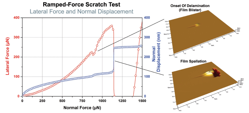
Figure 4. Representative data from a nanoscratch test showing how the critical load was determined. Image Credit: Bruker Nano Surfaces
The device’s capacity for in-situ SPM imaging was employed to successfully capture a topographical image of scratches at various points in the test to verify that the original critical event corresponds to film delamination, and that the far larger event that follows is a result of film spallation.
It is imperative that any instrument used to undertake tests such as these is capable of accurately detecting the relatively subtle onset of delamination, rather than the far more noticeable film spalling event.
A series of 1,884 nanoscratch tests were conducted on the wafer to effectively map the ULK film’s interfacial adhesion across the surface. As Figure 5 illustrates, substantial variation in film adhesion from one side of the wafer to the other was discovered. Additionally, over the majority of the wafer, adhesion was found to be distinctly lower within ~20 mm of the wafer edge.
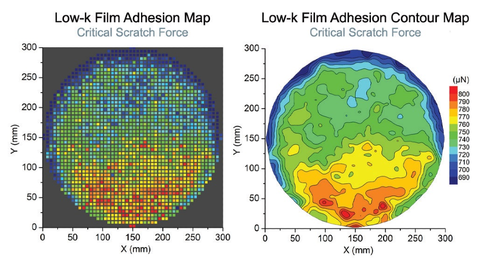
Figure 5. Results of 1,884 scratch tests on a 200 nm ULK film, showing adhesion variability due to non-uniform processing conditions. Image Credit: Bruker Nano Surfaces
Conclusions
As the examples above clearly highlight, today's leading nanomechanical metrology systems are able to help semiconductor manufacturers precisely balance the adhesion, mechanical, and electrical properties of ULK dielectrics. As nodes continue to advance, employing instruments like Bruker's ATI 8800 will ensure device reliability as well as uninterrupted production yield.
References
- W.C. Oliver and G.M. Pharr, J. Mater. Res., 7, 1564 (1992).
- R. Nay et al., Microelectronic Engineering, 75, 103-110 (2004).

This information has been sourced, reviewed and adapted from materials provided by Bruker Nano Surfaces.
For more information on this source, please visit Bruker Nano Surfaces.