The Universal Scanning Interferometry (USI) measurement mode has been recently released by Bruker to provide universal measurement results on a broad range of surfaces for ContourX white light interferometry (WLI) profilometers.
USI enables self-sensing, fully-automated surface texture optimized signal processing while offering the most realistic and accurate computation of the analyzed surface topography.
This article outlines how USI technology spans a wide range of applications, from semiconductor manufacturing metrology to advanced research and the inspection of medical components.
Technology Overview
No operator input is required in the USI technique, which automatically modifies algorithm parameters for ideal results on various surface textures in the same field of view, even on surfaces with differing heights, contrast, and intensity.
The USI is distinctive as it can be configured to automatically detect the surface type and to deliver the most precise areal metrology depiction of that surface.
As one of the most vigorous measurement methods within optical-based profilometry, the USI offers a single-measurement mode that integrates a vertical range of up to 120 microns with subnanometer vertical resolution metrology on almost all surfaces, whether opaque or transparent.
Multiscale data can also be acquired using this mode as subnanometer vertical resolution is maintained across the complete vertical measurement range. As an example, Figure 1 presents a cell phone camera lens measured after being installed into the assembly.
The wide scanning range enables the sides of the lens to be measured. The USI’s automatic surface sensing clearly shows the mold pin cylindrical grinding marks in the final image once the sphere shape has been automatically removed.
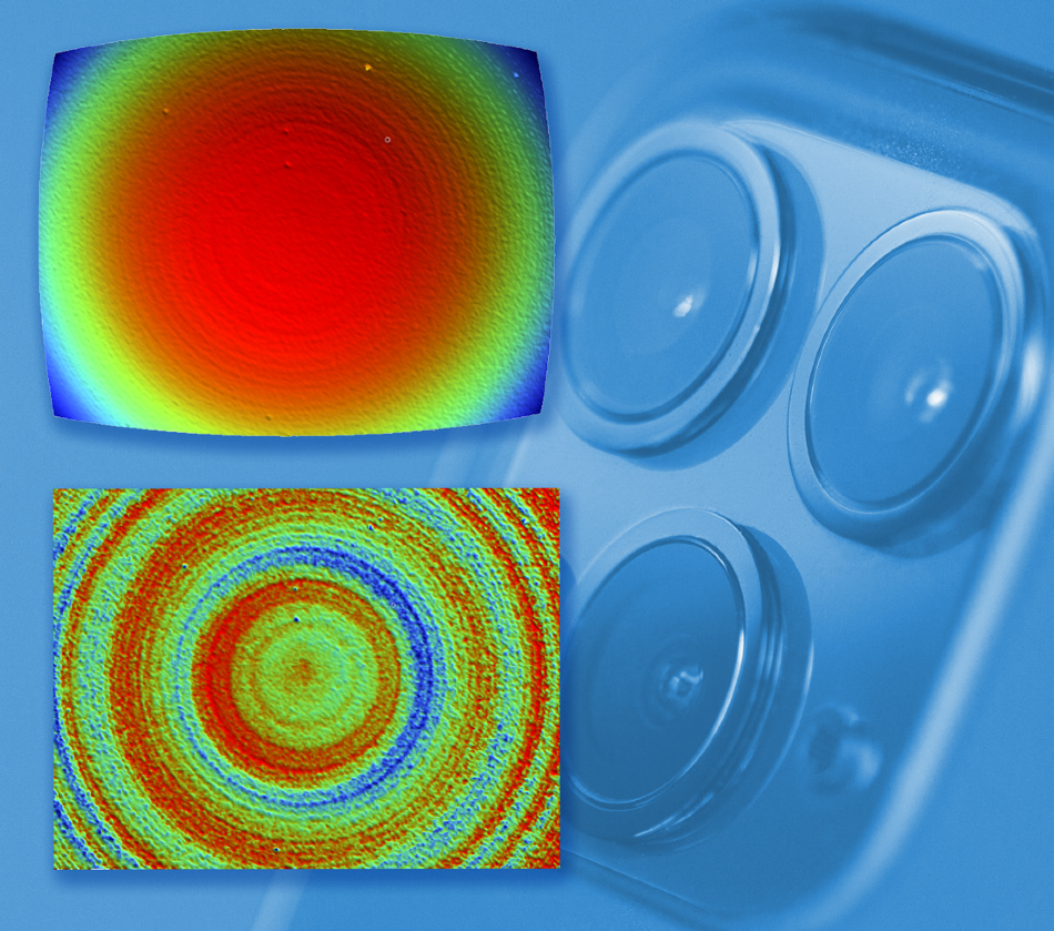
Figure 1. Camera lens measured (top), and with sphere shape removed (bottom). Image Credit: Bruker Nano Surfaces? and Metrology
Flexibility for a Broad Range of Applications
When characterizing various samples or in the case of multiple users, USI includes all of Bruker’s ease-of-use features while maintaining precision and accuracy for any surface being analyzed through auto selection.
To configure a continuous response in industrial inspection or to maintain testing and flexibility in advanced research, the USI gives users the option to choose between four operational resolution modes: Auto, Standard, High Fidelity, or High Speed. These options for process resolution can be selected by the user for various scenarios and is presented in a basic drop-down menu (shown in Figure 2).
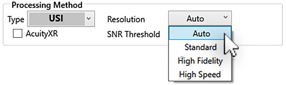
Figure 2. USI resolution modes. Image Credit: Bruker Nano Surfaces? and Metrology
The four main resolution settings are described below.
- Auto - The surface texture properties will be automatically detected by the 3D WLI metrology profiler and the resolution setting will be adjusted to one of the three other modes depending on the frequency or amplitude of the spatial topography.
This setting will default to High Fidelity for relatively smooth surfaces. Standard resolution will be used if the surface is less smooth to turn the surface signal data into a topography map with a balance between High-Speed mode and resolution. The system will select High Speed mode for rough surfaces with sudden and significant fluctuations in topology.
- Standard - Mainly used for smooth surfaces with subnanometer vertical resolution, this processes the surface measurement signal according to phase with a speed-enhanced algorithm.
- High Fidelity - Useful when the application demands the best possible vertical resolution (0.1 nanometer) even on diffuse or rough surfaces, this is another phase-based algorithm which will analyze the scan several times to attain the optimal and most precise data.
- High Speed - This has a stronger accuracy compared to previous vertical scanning algorithms as a center of mass (COM) enhanced algorithm. The most efficient USI measurement results can be achieved by this setting with nanometer precision and it is mainly beneficial when surfaces are comparatively rough with big steps.
These settings benefit all magnifications, including lower ones, to attain angstrom surface resolution on large height properties. This means that USI is appropriate for high submicron lateral resolution (high) along with large fields of view (wide).
Automatic sensing has been developed to balance speed of processing and acquisition with the highest quality data in relation to a given magnification or surface. Users can then completely focus on data generation or research while understanding the best results will be achieved each time.
In examples where the condition of the surface is well characterized, the user is given the choice to process the data in the fastest way possible, for example the high-speed option acquires data in the most efficient manner, with a slight decrease in vertical resolution.
Along with the resolution setting, the USI provides a signal-to-noise ratio (SNR) threshold setting, which excludes information with limited or low quality to capture high-fidelity topography.
The SNR threshold setting intelligently uses phase and average modulation data to present a quality ranking in percentage to further enhance reliability across a range of sample types.
Any specific data pixels which do not meet the minimum specifications will be excluded as noise and will be omitted from the final image, producing a reliable dataset without user input.
A 0 setting does not reject data while the best-tested setting is 2. The USI delivers multiple significant metrology advantages to Bruker WLI profilers as it can directly quantify the surfaces of semi-transparent materials.
For example, data storage and semiconductor manufacturers often employ alumina or dielectric to function as an insulating barrier between the conductive materials.
The majority of optical fringe height measurement algorithms are established on the center-of-mass computations from the camera signal frames returning from the surfaces. This means that when signals are received from the bottom and top surfaces of a transparent film, these heights are averaged at a location in the middle to provide the average height.
On a Bruker profilometer, selecting the appropriate USI mode enables the operator to choose the strongest signal out of both surfaces. This can be used as the measurement surface for height compared to alternative non-transparent conductive surfaces (shown in Figure 3).
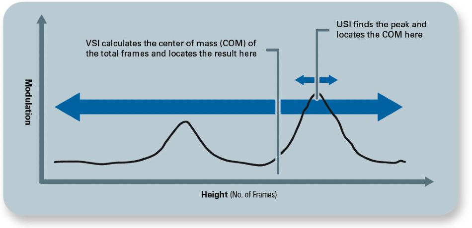
Figure 3. Schematic showing how the new USI mode provides more accurate and higher fidelity topography on transparent or challenging surfaces, as opposed to legacy modes, such as vertical scanning interferometry (VSI). Image Credit: Bruker Nano Surfaces? and Metrology
This direct surface measurement means the USI is an optimal non-contact measurement technique for these fragile materials for process control in lapping, deposition, and etching procedures.
Advanced AcuityXR® measurement methodology can additionally be employed with USI for the highest possible lateral resolution available for a specific field-of-view and magnification combination.
AcuityXR enhances lateral repeatability and enhances edge detection three to five times more than traditional microscope imaging for similar measurement parameters, as shown on the 1200 lines per millimeter grating in Figure 4.
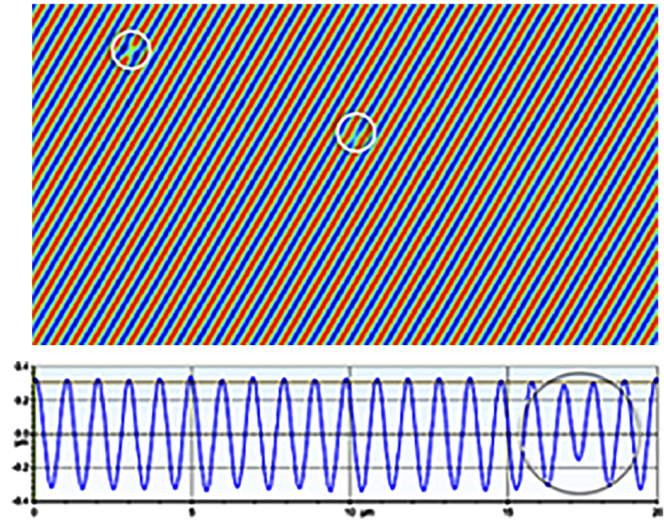
Figure 4. Submicron defects on 1200 l/mm polymer grating (39 µm by 21 µm). Image Credit: Bruker Nano Surfaces? and Metrology
Combining Large Step Height with Precision Surface Resolution
The USI is perfect for the characterization of any surface, from rough, steps, smooth, or a mixture of surfaces in a single image. The versatility of USI is demonstrated in Figure 5, which portrays the analysis of a chrome-on-glass lateral resolution standard (Siemens Star).
This standard integrates the imaging challenges of the differences in reflectivity in the two materials and the diffraction limit for a 10x objective.
The USI can reach the lateral resolution of the standard up to the physical limits, and precisely quantifies the hundreds-of-nanometers step height while measuring the glass substrate’s surface finish down to the angstrom areal Sa level with no requirement for filtering.
The USI is ideal for a variety of applications with its ability to create such a high-fidelity depiction of a highly dynamic surface structure.
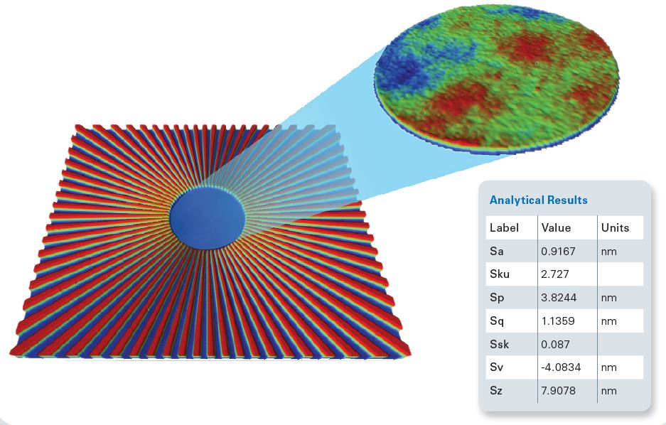
Figure 5. Resolution glass with angstrom surface finish. Image Credit: Bruker Nano Surfaces? and Metrology
MEMS and Microfluidics Applications
Figure 6 presents a closer view of a 3D interactive representation of a microfluidic device which is a testament to the data quality acquired with the USI technology from Bruker. The width and depth characterization of these channels is highly important as these microfluidic tools are normally employed to provide a very small amount of precise liquids.
USI provides diffraction-free images without the effects observed in alternative optical measurement devices when characterizing sharp-edged, high-sloped stepped structures with micron-deep smooth surfaces.
The USI processes this surface topography with ease and delivers high-quality, accurate data of the analyzed surface, which enables simple characterization of the essential depth, volume, and surface finish design function parameters of these tools.
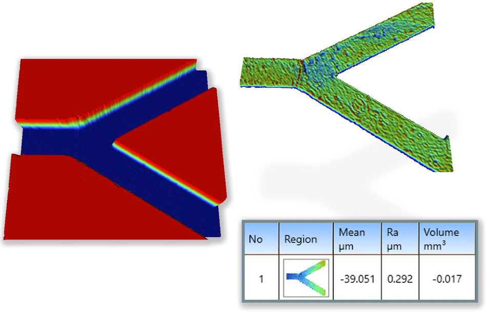
Figure 6. Analysis of the bottom channel of a microfluidic device with direct extraction via Multiple Region from Vision64. Image Credit: Bruker Nano Surfaces? and Metrology
Semiconductor and Wafer Manufacturing
The data storage industry continues to heavily depend on the production of traditional hard drives. With cloud storage fueling most of this demand, they are increasing the areal density storage limits with novel technologies, for example, EAMR, MAMR, and HAMR.
As this technology develops, a range of historic slider measurements continues to be essential, for example the characterization of the air bearing surface (ABS).
An air-bearing layer is created between the spinning magnetic media and the read/write head (slider) by the ABS surface. This enables the slider to hover above the surface without making contact, while generating a suction to contain the slider within a consistent nanometer height to optimize reading and track writing performance.
Figure 7 presents the USI characterization of the slider ABS step features, depicting hundreds-of-nanometers feature heights while depicting the subnanometer surface finish of the lower etched cavity and upper air bearing feature with angstrom repeatability, all in one measurement scan.
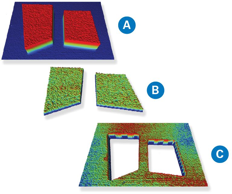
Figure 7. WLI images showing (a) HD sliders with ABS feature, (b) just ABS, and (c) cavity with subnanometer surface finishes. Image Credit: Bruker Nano Surfaces? and Metrology
The semiconductor industry uses a planarization or chemical mechanical polishing (CMP) process to smooth surfaces of the wafer with a combination of mechanical and chemical forces.
At different stages in the manufacturing procedure, wafer CMP is carried out for the removal of excess material to flatten the surface or reveal underlying features prior to adding the subsequent layer of circuit features.
The CMP process is performed across the entire wafer, which comprises various materials that planarize and wear at varying rates. Erosion (the feature’s depth) and non-proportional dishing (the surface’s curvature) are standard results of the CMP process, which can be observed in the excessive planarization presented in Figure 8.
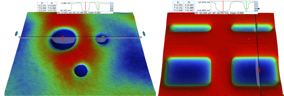
Figure 8. A CMP process resulting in dishing and depth differences. Image Credit: Bruker Nano Surfaces? and Metrology
Not only does this demonstrate the softer metal material curved or cupped from the CMP technique, but USI additionally characterized the depth and the shape of the larger feature with ease, which is approximately 10 nanometers deeper than the smaller attributes.
The semiconductor industry also has a range of inspection stages to validate the correct manufacturing of the wafer components and features. Figure 9a portrays a repeating wafer die structure that requires inspection, with no significant visual defects observed in this measured die.
Figure 9b presents an adjacent repeating die structure observed through the Vision Multiple Region software by Bruker, which automatically inspects and detects these differing types of structures.
The Multiple Region setting automatically detects these structures and flags the abnormal ones utilizing pass/fail criteria in the database logging.
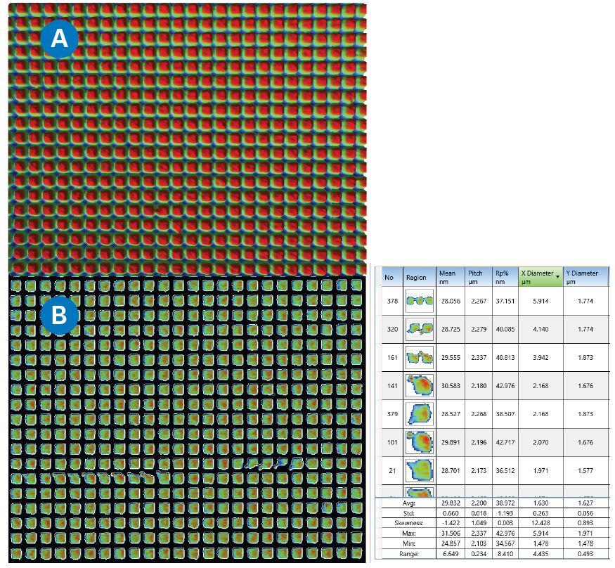
Figure 9. Wafer damascene structure (a), and wafer structure defect inspection (b) with Multiple Region setting. Image Credit: Bruker Nano Surfaces? and Metrology
Detection of larger regions can be performed where required by stitching several images together into a single large image of a complete die. Another technique performs like stitching where each separate image is measured during image acquisition for a range of pass/fail criteria, where failed images can be binned for additional analysis.
Precision Surface Machining and Roughness
Precision machining is a procedure where parts are manufactured under very restrictive tolerances to confirm that the technical GDT callouts for fit and finish and all specifications are achieved during the process of manufacturing.
Due to its nanometer sensitivity and wide field of view, a WLI profiler with USI measurement mode can provide more advantages compared to alternative measurement methods to achieve these meticulous design specifications.
Figure 10 presents an example of this, where two surfaces, one produced through grinding and the second vertically milled, yielded approximately 300 nanometers average roughness (Ra) when analyzed using a stylus profilometer.
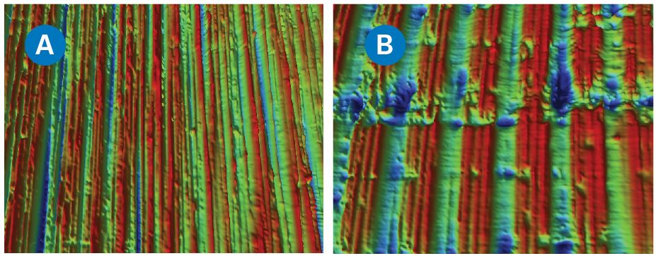
Figure 10. 300 nm Sa ground (a) and milled (b) surfaces. Image Credit: Bruker Nano Surfaces? and Metrology
USI measurement mode corresponds to the 2D stylus measurement (ASME B46.1 / ISO 4287) but can additionally present the distinct variations between these surfaces and can measure the differences utilizing the modern and globally renowned areal roughness S-parameters (ISO 25178).
Precision machining is conducted on a range of materials, such as bronze, steel, plastic, glass, and graphite, to name only a few. The resulting complex components and parts are employed in industries from aerospace to medical and automotive, covering almost all industries and technologies.
The WLI from Bruker with the single-measurement USI mode can quantify all of these surface finishes and materials, as shown in Figure 11 by the images of a tens of microns Sa milled surface and a precision nanometer Sa lapped-mated sealing surface.
The effective characterization of these surfaces proves that this technology makes iterative control possible across the finishing stages.
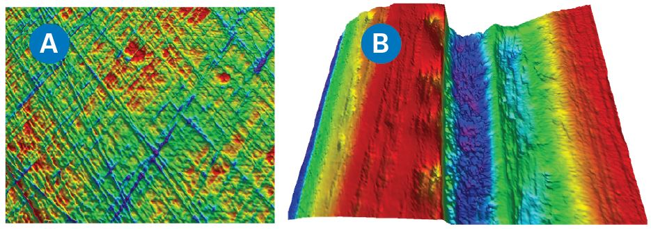
Figure 11. Nanometer Sa sealing surface (a) and tens of microns Sa milled surface (b) viewed with USI mode. Image Credit: Bruker Nano Surfaces? and Metrology
Conclusion
The Bruker optical WLI profiler’s USI measurement mode supplies users with significant benefits in metrology, including flexibility, ease of use, and a wider analysis range.
This self-learning, non-contact, universal measurement mode provides the most accurate 3D surface topography metrology available for the broadest selection of surfaces.
As outlined, the USI delivers accurate, efficient results able to provide notable details for applications ranging from precision machining and medical samples to data storage, semiconductor wafer device measurements, and MEMS.
These measurements are achieved with multiple images to cover larger regions or a single, quick measurement. This development in 3D metrology measurement delivers the most precise depiction of the range of different technical surfaces present in the current market.
Acknowledgments
Produced from materials originally authored by Roger Posusta and Samuel Lesko from Bruker.

This information has been sourced, reviewed and adapted from materials provided by Bruker Nano Surfaces.
For more information on this source, please visit Bruker Nano Surfaces.