InSight WLI is an inline, high-precision 3D optical profilometer developed for semiconductor applications that prioritizes accuracy, productivity, and process insights. This method uses white light interferometry (WLI) to detect lateral critical dimensions (CD) and topography depths quickly and without contact.
This cutting-edge technology includes 3D topography, CD metrology, and overlay measurements, allowing for sub-angstrom precision and step heights of hundreds of micrometers. InSight WLI offers full industrial automation, including SECS/GEM compatibility for 200 mm and 300 mm wafers, Cognex pattern recognition, and over 35 built-in analyses.
Image Credit: Bruker Nano Surfaces and Metrology
Only InSight WLI Delivers:
- Complete automation for high-volume production
- Versatile precision from nano to millimeter scale
- An integrated platform with comprehensive metrology coverage
Proven Performance for Inline Production
For many years, Bruker has offered superior optical profiling solutions to semiconductor fabs worldwide. Their sophisticated tools and local support ensure maximum uptime.
They ensure the technology aligns with the semiconductor roadmap and next-generation nodes. InSight WLI leverages extensive experience and cutting-edge technology to improve data reliability and streamline procedures.
Specialized and Proprietary Technology
InSight WLI utilizes industry-leading technology to support several applications, including FEOL, BEOL, advanced packaging, and MEMS. Using a laser reference for self-calibration during operation improves accuracy and maximizes uptime. Bruker's innovative automated tip/tilt head and specialized piezo scanners provide superior metrology performance for sub-nanometer roughness and nanometer critical dimensions.
Large-area scanning with stitching supports full-die imaging. SECS/GEM compatibility provides a smooth interface with host systems. Due to its advanced features, InSight WLI is a top metrology tool for semiconductor manufacturing and R&D.
A Mode for Every Surface
The three main measurement modes used by InSight WLI are PSI, VSI, and USI. These modes span a broad range of background noise, measurement time, and height difference. Intensity-based CD and overlay or film measurement modes for thin or thick films are examples of specialized modes for particular purposes.
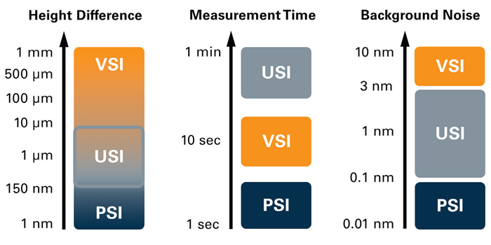
Image Credit: Bruker Nano Surfaces and Metrology
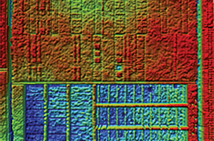
IC topography. Image Credit: Bruker Nano Surfaces and Metrology
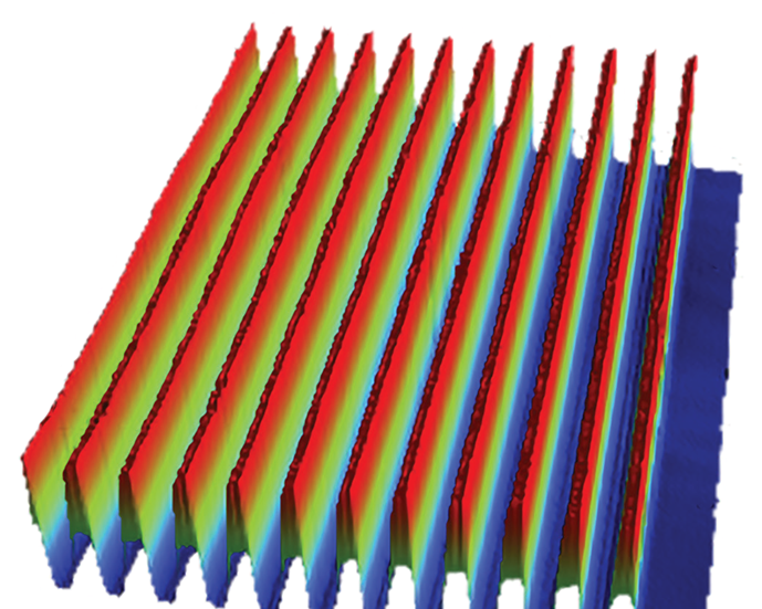
1 μm trenches. Image Credit: Bruker Nano Surfaces and Metrology
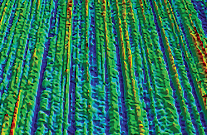
Sub-micron roughness. Image Credit: Bruker Nano Surfaces and Metrology
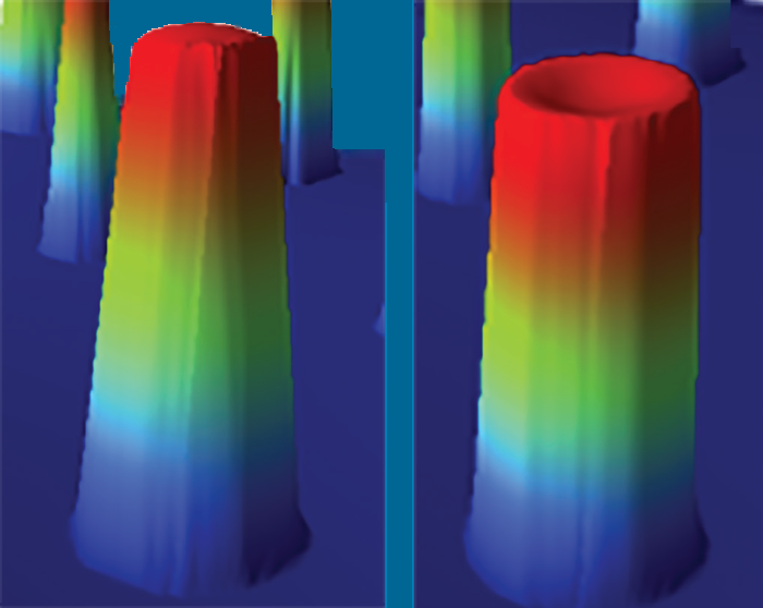
Copper TSV fill protrusion and micro-bumps. Image Credit: Bruker Nano Surfaces and Metrology
Micro-mirrors. Image Credit: Bruker Nano Surfaces and Metrology
Unmatched Application Versatility
InSight WLI offers exceptional features and capabilities for precise, repeatable measurements and analysis in FEOL, BEOL, advanced packaging, and MEMS applications. Fast and non-destructive technologies are used to measure surfaces such as warped wafers, high aspect ratio trenches, and ultraflat surfaces.
Effortlessly measure and analyze HAR TSVs on InSight WLI, such as the challenging 1:15 AR TSVs shown to the left. Image Credit: Bruker Nano Surfaces and Metrology
Achieve nanoscale accuracy in top and bottom CD measurements with overlay monitoring using intensity data frames, ensuring unmatched precision and reliability. Image Credit: Bruker Nano Surfaces and Metrology
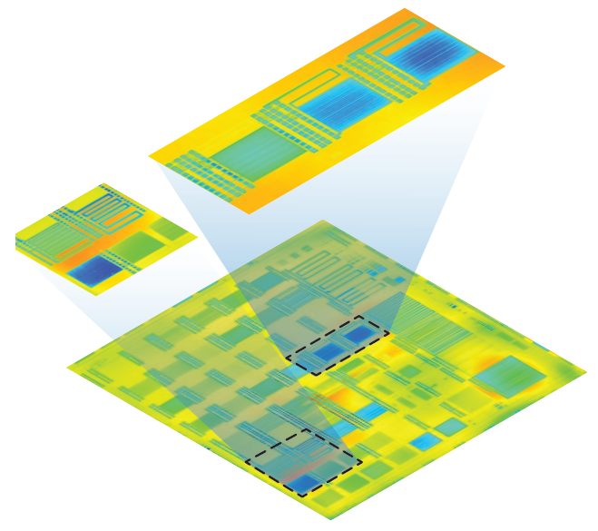
Seamlessly stitch large fields of view for critical hotspot detection, delivering unparalleled accuracy and performance. Image Credit: Bruker Nano Surfaces and Metrology
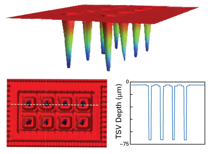
Through-Silicon Via and Through-Glass Via Monitoring
- Create 3D profiles for HAR TSVs up to 1:20 AR
- Ensure TSV quality using dependable methodology for 3D advanced packaging and CMOS image sensors (CIS)
Critical Dimension Monitoring
- Measure CD, profile, and edge roughness
- Maintain precise CD control for enhanced packaging
Overlay Monitoring
- Evaluate alignment between fan-out layers at the nanometer scale
- Obtain accurate overlays to optimize lithographic process windows
CMP Process Monitoring
- Measure post-CMP flatness, erosion, and flaws with high throughput
- Improve CMP uniformity through speedy and precise metrology
Die Flatness Qualification
- Stitch and inspect full dies for defects
- Ensure multi-chip modules meet flatness standards during wafer or die-to-wafer bonding
With Automated Metrology Capabilities
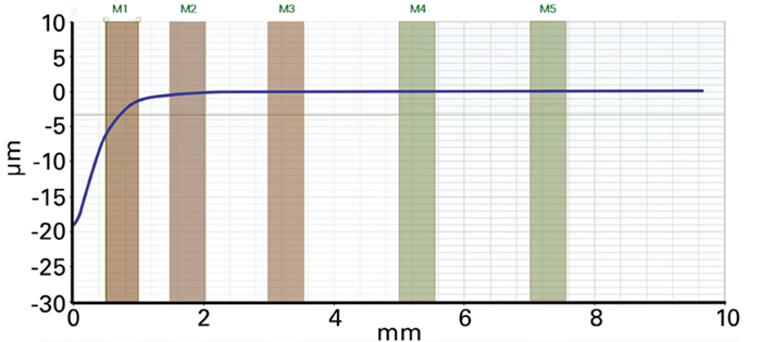
Experience high-speed, fully automated edge roll-off measurement with built-in analysis, extracting slope, Z-step height, and other key parameters, enhanced with edge detection. Image Credit: Bruker Nano Surfaces and Metrology
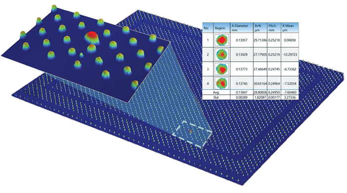
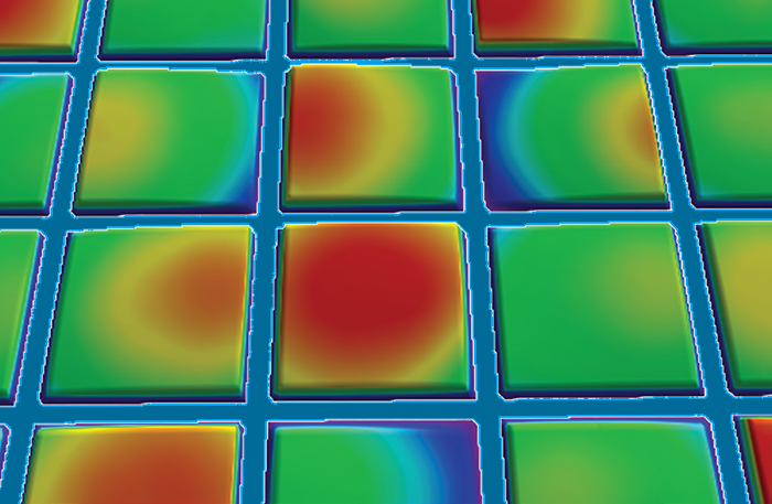
Full die bump array coplanarity and defect analysis with InSight WLI, ideal formicro bump and Cu pillar metrology, delivering sub-100 nm lateral precision. Image Credit: Bruker Nano Surfaces and Metrology
Etch Depth and Deposition Height Monitoring
- Measure depth and step height on a variety of substrates and metals
- Process monitoring for MEMS sensors and devices in high-power IC and legacy automotive application
Edge Inspection
- Automatically measure wafer edge roll-off (ERO) at radial points along the circumference of both bare and patterned wafers
- Monitor several edge parameters, such as slope, step height, and roughness
Bump Analysis
- Measure bump height, diameter, and pitch, and evaluate full-array coplanarity and flaws
- Monitor processes in packaging factories and electroplating equipment foundries
Superior Resolution, Accuracy, and Robustness
InSight WLI provides greater and more consistent vertical resolution than traditional non-interferometry-based optical profilers. It captures topography throughout the whole field of vision and calculates height independently for each pixel, resulting in faster results than other scanned optical beam technologies.
Unlike previous optical technologies, InSight WLI effectively separates interfaces on transparent layers up to 100 nm. The single optical head allows for full process monitoring and seamless transition between measurement modes, making it suitable for various applications.
White Light Interferometry As a Technique Has Several Inherent Benefits
- Vertical resolution is independent of field of vision or working distance. InSight WLI boasts an unrivaled vertical resolution limit of 0.01 nm
- The Sparrow criterion allows for lateral resolution as low as 0.38 μm while maintaining optimal resolution for each objective lens
- The universal application and resilience ensure precise measurements on surfaces with various properties, including translucency, reflection, and roughness
InSight WLI provides sub-nanometer vertical resolution and picometer precision for measurements ranging from nanometers to millimeters. This allows for precise investigation of semiconductor structures and surfaces with lateral resolution as low as 200 nm. Repeatability across measurement modalities ensures high confidence in outcomes.
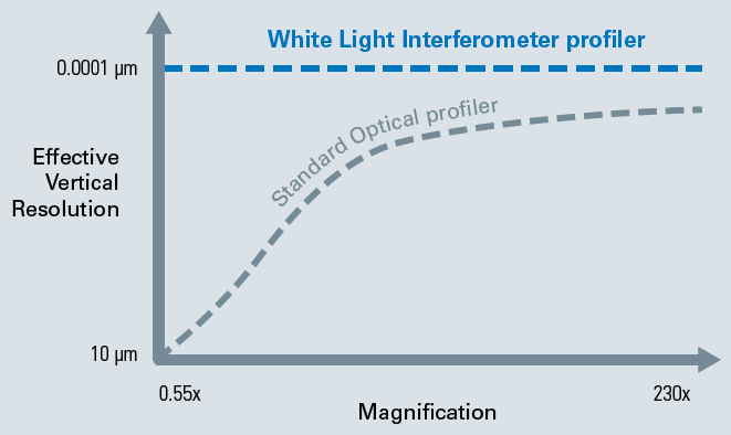
Effective vertical resolution is constant for WLI regardless of FOV, while it is variable for standard optical profilers. Image Credit: Bruker Nano Surfaces and Metrology
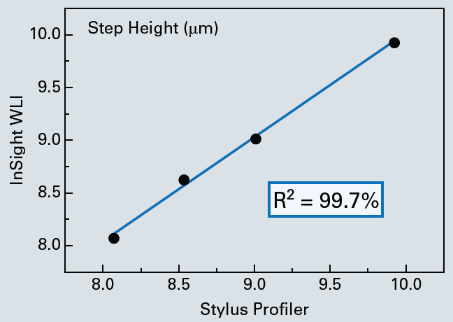
Regression/bivariate chart showing close agreement between InSight WLI and stylus profiler step height data. Image Credit: Bruker Nano Surfaces and Metrology
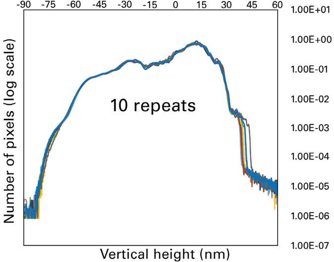
Height distribution from a full die. Ten repeats overlap very well, showing die flatness measurement down to 1 nm repeatability across the full distribution. Image Credit: Bruker Nano Surfaces and Metrology
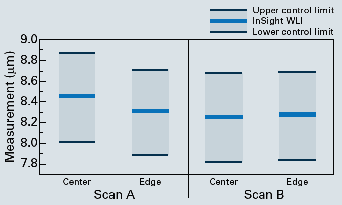
Accuracy chart confirming that InSight WLI measurements fall within the upper and lower control limits. Image Credit: Bruker Nano Surfaces and Metrology
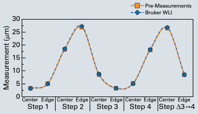
Measurement trend chart, tracking the excellent agreement between pre-measurements and WLI measurements. Image Credit: Bruker Nano Surfaces and Metrology
Advanced Automation and Analytics for HVM
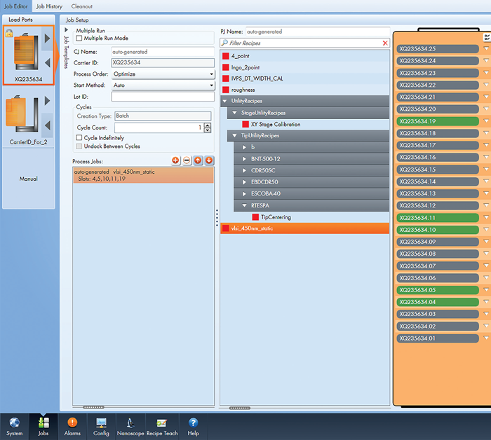
User interface for creating fully automated process job. Image Credit: Bruker Nano Surfaces and Metrology
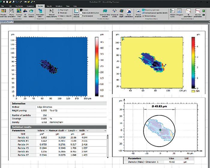
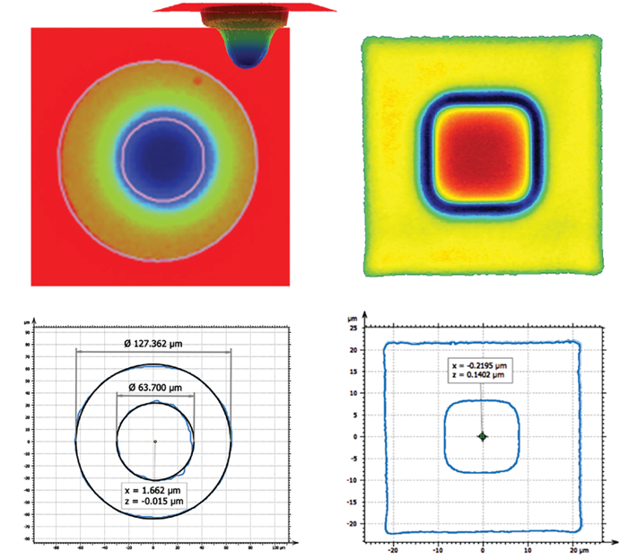
Vision64 Map probe mark diameter analysis. Image Credit: Bruker Nano Surfaces and Metrology
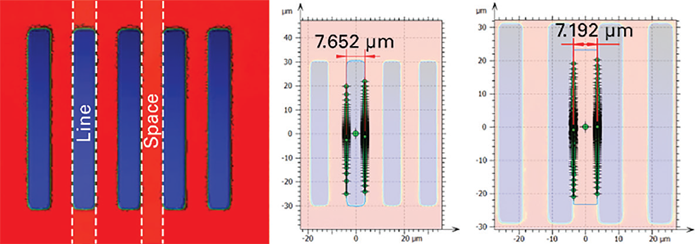
Line and space CD analysis using Vision64 Map. Image Credit: Bruker Nano Surfaces and Metrology
InSight WLI streamlines high-volume production processes from start to finish. It offers fast and consistent measurements with minimal operator intervention. Measurements can be easily set up using recipe development and automation capabilities, including autofocus, tip/tilt, and optional Cognex pattern recognition.
An EFEM shuttles wafers into the tool, where they undergo a pre-alignment procedure and have their wafer ID read. The wafers are positioned on a completely automated stage that can handle 200 mm or 300 mm wafers that are auto-loaded inline. Many wafer chucks are available, some designed to meet the requirements of certain applications.
Streamlined data processing includes rapid shape removal, automatic hotspot discovery, pass/fail database reporting, and over 35 built-in analyses. Optional Vision64 Map™ software offers sophisticated analysis and visualization capabilities, fully integrated with the tool's data for improved defect detection, correlation, and characterization beyond standard metrology requirements.
InSight WLI Select Specifications
Source: Bruker Nano Surfaces and Metrology
| . |
. |
. |
| Performance |
Vertical resolution |
Down to 0.01 nm |
| Lateral resolution |
Down to 0.38 μm (Sparrow criterion) |
| Vertical repeatability |
Down to 0.125% (1 σ) |
| System Hardware |
Wafer size |
200 or 300 mm, compatible with 300 mm fab automation |
| Wafer warpage handling |
Up to 4 mm |
| Chuck flatness |
Down to 1 μm flatness for 300 mm wafer size |
| Light source |
Patented dual-LED illumination (white, green) |
| Magnification |
Interferometric and Brightfield: 1.4x to 200x |
| Turret |
Encoded motorized 5-position turret |
| Camera resolution |
1200x1000 pixels |
| Optical path tip/tilt |
Patented automated goniometric correction up to ±2° |
| Vertical scan range |
Up to 1.5 mm |
| Measurement modes available |
Topography, film thickness, intensity-based lateral dimension |