 Interview conducted by Olivia FrostMar 4 2021
There are multiple ways to prepare samples for Electron Backscatter Diffraction (EBSD). The traditional and most widely used method is mechanical preparation, closely followed by electropolishing. Over the last five to ten years, people have been using focused ion beams for 3D EBSD. These were originally gallium FIBs, moving to plasma FIBs more recently.
The most recent tool is the broad argon beam, also called the broad ion beam, because it is possible to use ions other than argon. Gatan offers two broad argon beam products, a PECS II and an Ilion II, both of which can be used for preparing samples for EBSD. It should be noted that sample preparation requires a complete toolbox and a variety of tools because no single tool will do everything you need.
Our primary tool for EBSD is the PECS II, which stands for Precision Etching Coating System, II. PECS I sold for about twenty years, and PECS II came to market about five years later.
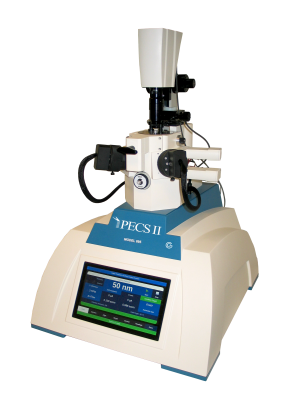
Image Credit: Gatan
The PECS I was mainly used for sputter coating very high-density films for electron microscopy applications. In PECS II, we have changed the tool's configuration because we saw a big need for EBSD compatibility, especially as EBSD has become prevalent with faster acquisition speeds and finer spatial resolution.
The PECS II tool can prepare very large areas, depending on how well the sample was prepared before entering the PECS II. Whether you are doing EBSD, cathodoluminescence, or high-resolution imaging of any sort, it is important to ensure repeatability from sample to sample.
Using an argon or an ion beam tool is an easy way to gain that advantage over some other techniques. The PECS II instrument has a very user-friendly interface. In our system, there are no icons, meaning there is no ambiguity in the function of each control. It is easy to use in English, but users can also push a button and switch to German, French, Russian, Korean, Japanese, traditional Chinese, and simplified Chinese, or back to English.
Why is mechanical polishing such an important and widely used sample preparation technique?
Metallography or mechanical polishing is one of the most widely used sample preparation approaches. While it is simple to do, it requires skill and patience to perform correctly.
In many cases, people have samples that they want to polish cross-sectionally; for example, a thin metal coating that is soft on its interface on a very hard metal or a sandwich-type structure with multiple layers of polymer and metal next to each other. This variation makes it hard to prepare from a mechanical point of view. Sometimes you must use chemicals, including acids, to remove a final damage layer, and automated polishing may not work all the way down to the finest polishing abrasives to prepare complete samples properly.
There may also be changes required in a recipe to accommodate small changes in the material, or even if the weather changes, or if you have two labs using city water and the pH of the water is different. We often need to shape the sample down to a reasonable size. This may require the use of a belt grinder followed by a very coarse polishing step and a further simple polishing step; for example, using a one-micron diamond or nine-micron diamond.
What factors should be considered when using argon or broad ion beam tools for EBSD preparation?
Argon is one of the noble gases along with xenon and neon. It is an inert gas, unlike gallium that is commonly used with a FIB. The gas being inert means that we do not see any chemical interaction with the material. Broad ion beam tools have reasonably high brightness and milling rate and a very low damage rate. The tool itself costs approximately ten times less than a FIB, but it does cost more than a suite of mechanical polishing tools.

Image Credit: Shutterstock/Oleksiy Mark
Some factors should be considered, however. Because we are working with an ion accelerated to low energy, this can still implant into the material or cause an amorphous layer. We must determine what we are using as a milling voltage and milling angle and how this might affect the results and the rate of removal of material.
The PECS II system is designed for ions, specifically neon, argon, and xenon, at very low energy. This instrument is not for high implantation energies but rather from 100 volts to 6 keV. It is useful for both SEM preparation of samples and also TEM, where people go to much lower energies.
For SEM work, we typically run between 4 and 6 keV. With samples that contain polymers or very soft material, we might go down to 2 or 1 keV. When working with the TEM, especially for post-FIB cleanup, we would go down to around 100 volts.
Overall, the lowest ion mass penetrates the deepest. The smaller ion will end up going deeper into the sample material while also having the largest straggle or spread. For example, neon’s error bars are much wider than those of xenon, so there will be a lot more spreading for better or worse, but it will also penetrate deeper, which may impact crystal lattice quality if you are trying to measure strain accurately.
The sputtering yield is an indication of how much material being removed. The sputtering yield can be understood as a function of energy, but it is not always clear about the best angle. If the beam is perpendicular to the sample surface, it is just driving into the sample surface, and there will be a very low sputtering yield.
If the beam goes to zero or very close to zero, it will glance off the surface, and there will not be much sputtering yield. There is a variation in the sputtering yield in the area that is important for SEM work. This is as low as 2 keV up to 6 keV, or 4 keV to 6 keV, which we usually use. Because of this, we typically run at angles between two and six degrees when we are doing this work.
There are reasons to run at higher angles at times; for example, the yield or sputtering rate varies as a function of material and the crystallographic plane that faces the sample surface. Users may want to utilize a small amount of preferential milling because it can actually show things like grain boundaries and tilt boundaries without affecting EBSD.
What are the advantages of using argon as opposed to xenon or other inert gases?
Plasma FIBs tend to use xenon because they require a higher sputter rate. They use a larger sized beam to prepare as large an area they possibly can. We can actually use xenon in the PECS II tool and in other broad argon ion beam tools. However, it is important to think about the amorphization layer when selecting which gas to use. This is a function of energy, and by moving the atoms from their preferred location in the lattice, you can make an amorphous layer.
There is a lot of data on the effects of energy rates below 1 keV, and this is where people are using broad argon beams with TEM samples. These typically run down to 100 volts because it is important to get the amorphous layer as close to zero as possible - usually, one or two nanometers, which still represents a reasonable percentage of the thickness of a sample, given this might only be 20 to 50 nanometers thick for TEM samples. The layer of thickness decreases with decreasing beam angle and is thinner for lower energy. For this reason, we tend to run at low angles most of the time.
Most users are trying to find a balance between sputtering off material and creating new damage, so they tend to run above 500 volts and at angles of about 10 degrees or less. This will produce the cleanest, lowest damage surface. From all perspectives, xenon is better, but companies are increasingly selling broad argon beam tools as opposed to broad xenon beam tools simply because xenon costs 500 to 1,000 times more than argon.
Our tools include two gas inlets, and these can be specifically calibrated to run xenon on the guns and argon or dry nitrogen in the purge system or to open and close the valves. Opening and closing the valves uses more gas than actually running the guns, so this balance works well for some customers. The sputtering rate in amorphous layer thickness varies with energy, and it is important to try to reach a steady state. If you know the energy and know the damaged layer thickness, it would double the time to remove the higher energy layer.
This is an important consideration because users frequently want to run a recipe much like they do mechanical polishing - going from coarse to fine polishing or high voltage to low voltage using a FIB. Some users may want to run a recipe that steps down from a higher accelerating voltage to a lower accelerating voltage and then perhaps to a higher angle just to do some delineation of the surface. The use of broad ion beams is ideal in these scenarios.
Can you give our readers some examples of how using a broad argon beam and the PECS instrument can help users obtain high-quality EBSD data?
Our product line offers several features designed to collect high-quality EBSD data, but effective sample preparation remains a key consideration.
It does not matter what benefits our analytical tools bring if the sample is not prepared well, and nothing else provides the quality downstream that matches what can be achieved with a good preparation approach. The samples highlighted here are samples that were difficult to prepare effectively using a traditional mechanical preparation approach.
While we have historically used mechanical preparation in our lab, we have begun to use ion beam applications more and more, particularly as we became more familiar with the technique and the advantages gained by using the PECS II and ion beam preparation.
The Velocity EBSD Camera series is based on a high-speed, low noise CMOS sensor. These have replaced CCD sensors as the primary tool used for EBSD collection. These cameras are ideal for in-situ and 3D-type experiments where collection speed is critical.

Velocity EBSD Camera Series
Image Credit: EDAX
In one example scenario, a multiphase aluminum alloy was prepared using the PECS II with an acceleration voltage of 4 keV, a tilt angle of 3 degrees, and an etching time of 20 minutes. With 500-nanometer steps and 20 keV acceleration voltage running at about 400 patterns per second, acquiring a complete map would take about 8 minutes.
SEM secondary electron images of the sample taken before polishing with the PECS reveal that different phases are present, but when the beam is tilted to 70 degrees for EBSD work, a traditional polishing approach does not give useable EBSD patterns from all phases.
Aluminum generally provides good EBSD patterns, but the tin patterns are much weaker and much more diffuse.
PRIAS is an approach whereby the EBSD phosphor screen is used in parallel with the EBSD collection as an electron detector. To operate as an electron detector on the SEM, we monitor the signal flux in different regions of interest on the phosphor screen as we raster the beam across the area of interest. Reconstructing the differences in intensity as a set of images reveals different contrasts of interest, including orientation, atomic number, and topographical contrasts.

Pattern Region of Interest Analysis System (PRIAS)
Image Credit: EDAX

EBSD patterns from the aluminum and tin phases prior to ion beam preparation, with weak tin patterns observed. PRIAS (center ROI) and Inverse Pole Figure (IPF) orientation maps also shown.
Image Credit: EDAX/Gatan
In the example here, the PRIAS image shows us a sort of a molting effect within some of the grains. We compared this with an IPF orientation map, and this showed a color change in those grains. This was essentially an artifact that had occurred during the mechanical polishing.
The artifact was orientation-dependent, which was not visible in all the grains and not representative of the material's true microstructure.
We also noted that the tin particles were more speckled colors. This was where we were not getting reliable indexing, which was confirmed by lower Confidence Index values. We were also able to see that additional deformation had occurred next to these particles, likely due to a differential polishing rate between the two materials.

EBSD patterns, PRIAS (Center) map and IPF orientation map after PECS II polishing. Now the tin areas can be indexed successfully and the artifacts observed earlier removed.
Image Credit: EDAX/Gatan
After 20 minutes of ion milling, it was possible to see a nice, clear visual representation of the microstructure. The tin grains were now smooth. The sample at a 70-degree angle for EBSD reveals darker grains, while the silicon grains are etched somewhat and recessed slightly down below the prepared surface plane. This was a much more useful surface when we looked at the improvement of the EBSD patterns for all phases. The aluminum patterns were much sharper, and we acquired much better EBSD patterns from the tin phase. The aluminum grains’ molting had also gone away.
How important is it to use a sample preparation approach that can also accommodate secondary phases?
This approach provides higher indexing rates for all the phases. This is important, especially for samples like aluminum alloys where the mechanical polishing tends to focus on the primary matrix phase, meaning it is harder to get usable EBSD patterns from the secondary phases present in a lot of real-world samples. Ion beam preparation allows us to get useful diffraction data from these phases.
What are the benefits of using a Hikari Super Camera with the PECS II instrument?
The Hikari Super Camera is a CCD-based camera capable of speeds up to 1,400 points per second. Its approach is similar to the CMOS-based Velocity in terms of how the indexing engine works, but the Hikari is an older camera based on CCD technology.
Looking at an amalgam sample prepared using a 6 keV, 2 degree glancing angle for 90 minutes, then followed with EBSD collection using a Hikari at 70 nanometers steps, 20 keV, 100 points a second, allowed the collection of around a million data points, even when working with a sample that was looked at without any initial preparation. This collection speed was selected to allow for collection of simultaneous EDS-EBSD data with good collection statistics.
Looking at the sample with the backscatter detector prior to preparation, it was hard to recognize any individual phases or structures, and there were no EBSD patterns obtained on the as-received sample.
PECS II was used and, looking at the sample under equivalent conditions, it was possible to see that the surface had been smoothed out significantly. It was possible to see the microstructure.
The EBSD maps revealed several different phases; a mercury silver phase and a copper-silver phase were detected. Using EBSD, it is possible to resolve the different grains and their grain orientation to see if there is a preferred orientation.
The phase map distribution showed the red, green, and yellow color-coded phases combined in a single map. We were able to compare that to the PRIAS images to confirm that patterns from all the different phases are present.

IPF on PRIAS center map and phase distribution on IQ map of an amalgam sample. The PRIAS images and patterns show the three phases. This was made possible by using the PECS II to polish the sample, resolving very fine features in a complex microstructure.
Image Credit: Gatan
Overall, utilizing an ion beam helped us go from a surface where EBSD revealed no features to resolving very fine features in a complex microstructure.
The PECS II is ideal for use with a range of samples that are difficult to prepare traditionally. It is very easy to operate, and it is very effective, even when investigating samples that have oxidized, have deformation, or have irregular surfaces.
The PECS II allows users to prepare a surface suitable for doing good EBSD work. It can also be used on large areas or with difficult materials, for example, strained, soft, porous, or multiphase materials.
The PECS II does not require expert knowledge to be able to achieve excellent results. It is an easy push-button tool that allows users to get the results they need.
About EDAX
EDAX is the global leader in Energy Dispersive X-ray Spectroscopy (EDS), Electron Backscatter Diffraction (EBSD), Wavelength Dispersive X-ray Spectrometry (WDS) and X-ray Fluorescence (XRF) systems. EDAX manufactures, markets, and services high-quality products and systems for leading companies in semiconductors, metals, and geological, biological, material and ceramics markets.
EDAX is a unit of AMETEK Materials Analysis Division. AMETEK, Inc. is a leading global manufacturer of electronic instruments and electromechanical devices. AMETEK is divided into two operating groups, the Electronic Instruments Group and the Electromechanical Group. The Electronic Instruments Group consists of four market groups: Process & Analytical, Aerospace, Power, and Industrial.
The AMETEK Materials Analysis Division is part of the Process & Analytical Group and is comprised of seven business units Advanced Measurement Technology, AMPTEK, CAMECA, EDAX, Gatan, SPECTRO and VISION RESEARCH, each of which is technology and quality leaders in their markets.
About Matt Nowell
Matt is the EBSD Product Manager at EDAX and has a passion for EBSD and microstructural characterization. Matt joined TexSEM Labs (TSL) upon graduation from the University of Utah in 1995 with a degree in Materials Science and Engineering. At TSL, he was part of the team that pioneered the development and commercialization of EBSD and OIM. After EDAX acquired TSL in 1999, he joined the applications group to help continue to develop EBSD as a technique, and integrate structural information with chemical information collected using EDS.
Within EDAX, Matt has been involved in a number of roles, including product management, business development, customer and technical support, engineering, and applications support and development. Matt has published over 70 papers in a variety of application areas. He greatly enjoys the opportunity to interact with scientists, engineers, and microscopists to help expand the role that EBSD plays in materials characterization. In his spare time, Matt enjoys playing golf and pondering if changing the texture of his clubs will affect his final score.
About Micheal Hassel Shearer
Michael Hassel Shearer has a Ph.D. in Materials Science from Carnegie-Mellon University. Previous to working at Gatan, Mike worked at JEOL as Semiconductor Equipment Product Manager for 27 years. He has been at Gatan for 11 years, where he is Product Manager for Sample Prep Equipment.

This information has been sourced, reviewed, and adapted from materials provided by EDAX, LLC.
For more information on this source, please visit EDAX.
Disclaimer: The views expressed here are those of the interviewee and do not necessarily represent the views of AZoM.com Limited (T/A) AZoNetwork, the owner and operator of this website. This disclaimer forms part of the Terms and Conditions of use of this website.