Thin films with desired mechanical, electrical, and optical properties are ubiquitous in modern life. The deposition of such advanced thin films, especially on small parts with complex shapes, is a challenging process requiring complex development and verification activities.

Image Credit: TOFWERK
Employing a fibTOF secondary ion mass spectrometer is an effective means for depth profiling of thin films.
The instrument is able to provide vital information about the elemental composition of the layer structure; for example, details on the chemical homogeneity at the surface and in buried layers (such as an adhesion layer), detection of contaminants (typically found at the interface between two layers) and sharpness of interfaces between layers.
While secondary ion mass spectrometry has been used to analyze thin films for some time,1 the fibTOF has evolved this method through the provision of high-resolution chemical images and removing the need to select elements of interest prior to analysis.
This article outlines the use of fibTOF in two common examples of inorganic thin film measurements.
Example 1: A Vertical Cavity Surface Emitting Laser
Figure 1 displays a depth profile through part of a vertical cavity surface-emitting laser (VCSEL). This was constructed from five gain regions using epitaxially bonded AlGaInAs-InP and a distributed Bragg reflector of several alternating GaAs-AlAs layers.
A full description of these devices’ structure and operation is available elsewhere.2
Figure 2 displays an enlarged image of the aluminum depth profile. This has been superimposed on the device’s structure to illustrate structure within the gain regions.
This depth profile was obtained by using a fibTOF instrument to measure secondary ions generated via a focused ion beam microscope using Ga+ ions. This method used the VCSEL sample reported by Whitby et al.3
This approach successfully demonstrated depth resolutions better than 8 nm and lateral resolutions better than 25 nm. It should be noted that it is possible to detect even thinner layers of nanometer thicknesses, for example, adhesion layers of chromium, titanium, or titanium oxide.
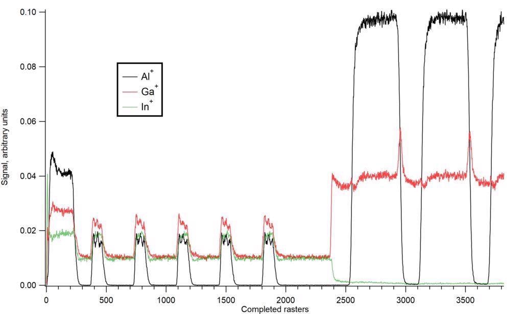
Figure 1. Depth profile through part of a vertical cavity surface emitting laser (VCSEL) obtained using Tofwerk’s fibTOF with a gallium ion focused ion beam microscope. For optimal depth resolution, the focused ion beam was used with a low energy of 3 keV. The various layers in the semiconductor stack can be clearly seen although the peak of the Ga+ signal between each Bragg reflector pair to the right of the image is an artefact of the sputtering process. The x-axis is given in completed rasters of the FIB microscope over the selected area; note that this is strictly proportional to depth if and only if the sputtering rate is constant (unlikely in a depth profile through different materials) and the current of the FIB beam is constant. Image Credit: TOFWERK
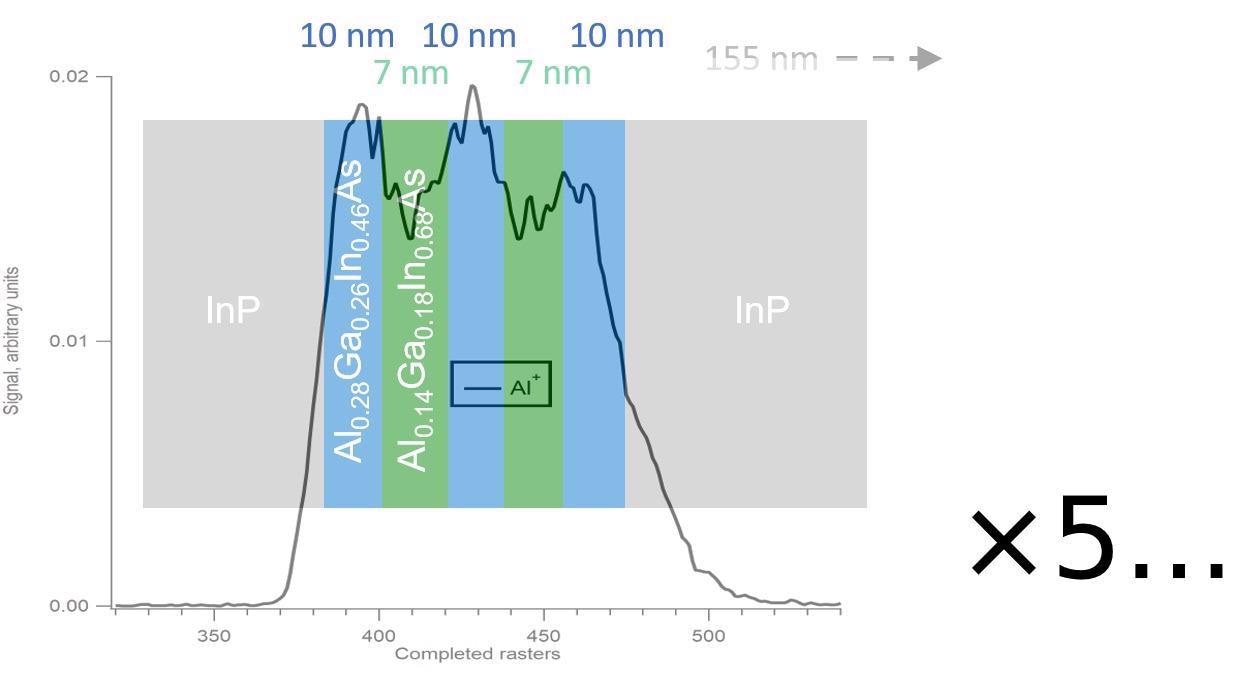
Figure 2. A zoom of part of the Al+ trace from Figure 1 (black line) superimposed on a schematic indication of the thin film layers that define the quantum well gain region of the VCSEL device. There are five such regions (see Figure 1) each consisting of three more aluminum-rich layers (indicated in blue) are each 10 nm thick, separated by 7 nm of a layer with less aluminum (indicated in green). The trace from the fibTOF SIMS measurements shows three peaks in the aluminum concentration as expected. Image Credit: TOFWERK
Example 2: Confirming the Presence of an Adhesion Layer in a Thin Film Stack
This example saw measurements acquired using a fibTOF being used to determine whether or not a titanium and/or platinum adhesion layer existed at the interface between a lithium tantalate substrate and a gold coating.
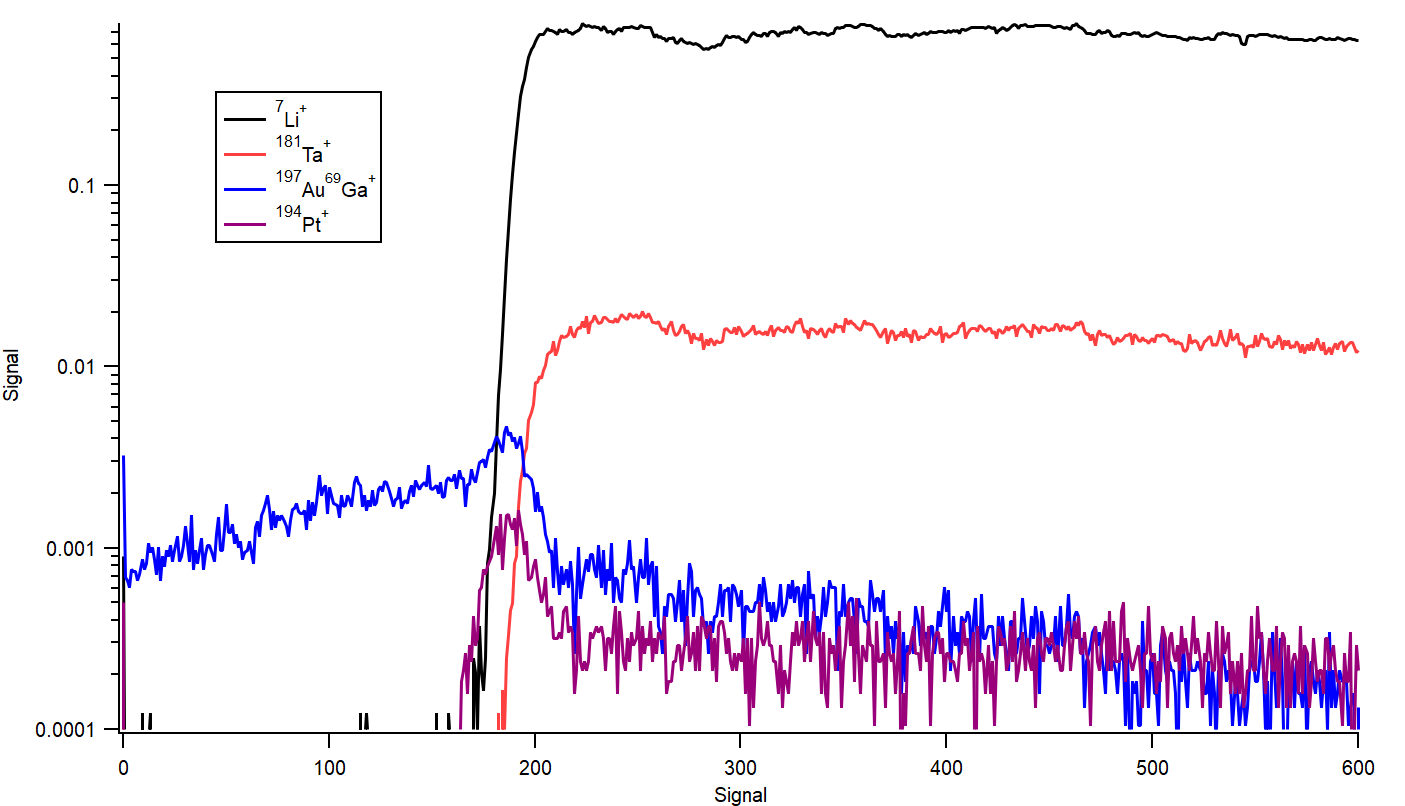
Figure 3. Positive secondary ion depth profiles for gold coated lithium tantalate. Image Credit: TOFWERK
This investigation did confirm the presence of a platinum adhesive layer between the gold coating and the substrate. The instrument was unable to completely resolve the signal from gold at m/q 197 because the amounts of TaO+ and the other isotopes of TaO were too low to be useful.
Thankfully, a priori information about the composition of the sample allowed for an unambiguous interpretation.
While it is advisable to approach analysis of mass spectral information with an open mind, it is also sensible to make use of any existing information about the sample or any details of typical contaminants in the measurement system.
The figure also shows another technique: the use of the adduct ion signal from GaPt+. In this material, this signal was stronger and therefore posed less risk of isobaric interferences than the Pt+ ion signal.
Advice for Assuring the Best Depth Profiles
In order to ensure optimum depth resolution, the focused ion beam should maintain the lowest energy possible while ensuring that the spot size is not increased so much as to reduce the shape quality.
When producing a depth profile from acquired data, it is advisable to adjust the lateral margins of the region of interest, only making use of data from the center of the pit. This helps avoid milled pits with sloping walls.
The crater’s floor should ideally remain flat, typically requiring adjustments to the focused ion beam, scan rate, pixel size, or beam current.
Under certain conditions, some materials milled by a focused ion beam may become rough or develop a wave-like surface.4 resulting in degradation of depth resolution.
This can be addressed via minor alterations of the stage angle, adjusting the beam conditions, or through the use an assist gas where a FIB-SEM instrument is equipped with a gas injection system.
Should a larger sampling area be required, it is recommended that measurements be obtained in several places to ensure that the thin film is homogenous; for example, at the center and edges of a wafer or close to and far from an ALD precursor inlet nozzle.
Complementary Methods for Thin Films Analysis
A number of complementary techniques can be used alongside FIB-SIMS when investigating thin films’ composition and structure. These include ellipsometry, X-ray reflectance, X-ray fluorescence, or glow-discharge profiling - as long as the layers remain homogenous on a scale of many millimeters.
Creating a cross-section of the thin films (mechanically or using the FIB) can offer additional insight into the layering structure. When working with thicker films, it may be prudent to employ techniques such as EDX or (near-field) Raman microscopy in order to obtain information about structure and composition.5
An atomic force microscope can also be used to measure the depth of FIB pits, providing accurate information about the depth of features observed in the depth profile.
References
- Zinner, E. Depth profiling by secondary ion mass spectrometry. Scanning 3, 1980. DOI: 10.1002/sca.4950030202
- Iga, K. Surface-emitting laser — its birth and generation of new optoelectronics field. IEEE J. Sel. Top. Quant., 2000. DOI: 10.1109/2944.902168
- Whitby, et al. High spatial resolution time-of-flight secondary ion mass spectrometry for the masses: a novel orthogonal ToF FIB-SIMS instrument with in situ AFM. Adv. Mat. Sci. Eng, 2012. DOI: 10.1155/2012/180437
- Shenoy, V. B. .; Chan W. L.; Chason, E. Compositionally Modulated Ripples Induced by Sputtering of Alloy Surfaces, Phys. Rev. Lett., 2007. DOI: 10.1103/PhysRevLett.98.256101
- Gucciardi, et al. Near-Field Raman Spectroscopy and Imaging. Applied Scanning Probe Methods, Springer, Berlin, Heidelberg, 2006. DOI: 10.1007/978-3-540-37316-2_10
Acknowledgements
Produced from materials originally authored by James Whitby and Lex Pillatsch from TOFWERK.

This information has been sourced, reviewed and adapted from materials provided by TOFWERK.
For more information on this source, please visit TOFWERK.