Biomedical technology has led the way in the utilization of microneedles for effective skin delivery. Manufactured from a wide range of materials, microneedles comprise vertical arrays of micron-sized projections.
They are designed to penetrate the epidermis (the outermost skin layer) and interface the epidermis and the second skin layer, the dermis.
Microneedle technology has been proven to enable improved transdermal delivery of active agents such as nanoparticles, small polar molecules and macromolecules that would otherwise be impermeable to the skin.
At present, microneedles are constrained by shortcomings, including uncontrolled degradation and limited drug loading capacity. Advancements in microneedles, such as the ability to size down to the nanoscale, offer incredible advantages.
Nanoneedles, in particular, are a promising development. These micron-sized needles integrate features at a nanoscale level and offer reduced invasiveness, increased surface area, plus pain-free administration.
The ability to manage control of the over degradation rate of micro/nanoneedles within the skin itself continues to be a significant challenge.
The development of porous silicon nanoneedles (pSiNNs) offers advantages in the treatment of a variety of illnesses, primarily due to their biodegradability, tunable porosity and mechanical strength for non-invasive drug delivery.
By using an Oxford Plasma 100 deep reactive ion etching (DRIE) instrument to manufacture nanoneedle arrays with a length of 40-50 µm and a tip diameter below 1 µm were fabricated. These sharpened nanoneedle projections are able to puncture the outermost layers of the skin, allowing the delivery of therapeutic agents.
The manufacturing process involves UV photolithography patterning, followed by a dry etching procedure utilizing a DRIE tool. The resulting nanoneedles are then posified via a wet etching process by electrochemical anodization.
Lithography
Nanofabrication of vertical arrays was completed using P-type, low resistivity silicon wafers as a starting substrate. The silicon wafer was coated with positive photoresist (AZ®4562) by spin coating before the substrate was baked at 110ºC.
A chromium mask was utilized to transfer the defined pattern onto the substrate by means of UV exposure. The last step of the process involved the photosensitive-coated substrate being immersed in AZ®400K developer solution.
This resulted in the exposed resist being removed, bringing the process of photolithographic patterning of nanoneedles to completion.
DRIE Process
Silicon wafers containing photoresist-patterned circles were etched utilizing an Oxford Plasmalab 100 DRIE. This was done by carrying out a Bosch process and then a standard dry etching base on RIE.
Fabricating nanoneedle arrays is a three-step process:
- Utilizing an isotropic sulfur hexafluoride (SF6) step to create a sharp tip
- Carrying out a Bosch process step to obtain cylindrical posts in an anisotropic etching
- Reshaping the nanoneedles with a mixture of octafluorocyclobutane (C4F8) and SF6 gases which give sharper tips for enhanced skin penetration
In the SF6 step, the sharp tip of the nanoneedle arrays was created by using an isotropic SF6 etching process with controlled time, whereby the flow rate of SF6 gas is adjusted, and the RF power and ICP generator power are maintained.
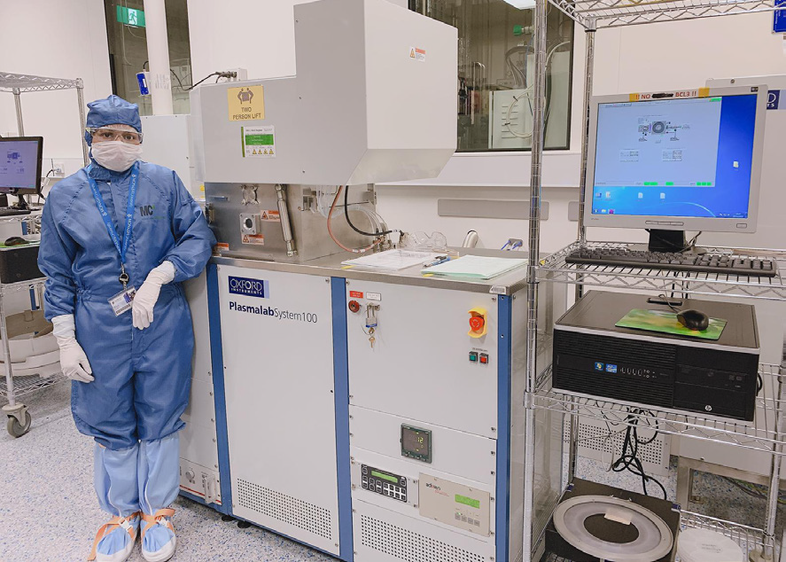
Image Credit: Oxford Instruments Plasma Technology
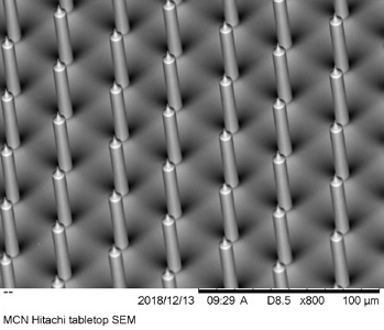
Image Credit: Oxford Instruments Plasma Technology
The Bosch etching process utilized SF6 in the etching cycle and C4F8 gases in the passivation cycles. The flow rate of C4F8 and SF6 was adjusted in both cycles.
Helium gas pressure was parametrized utilizing the APC valve position and table temperature values, while the required depth of Si etching was proportionally achieved by means of the etching and passivation cycles.
The photoresist on the tip of the nanoneedle array was later removed with isopropyl alcohol, acetone and water by means of a sonication bath. This process took approximately 1 minute for each solvent.
Porosification was achieved by utilizing electrochemical etching of the silicon nanoneedles. The silicon wafers containing nanoneedle arrays were electrochemically etched in a 3:1 volume ratio solution comprising hydrofluoric acid (48%) and ethanol, respectively.
Etching was performed at constant current density over a time period, giving a pSi layer thickness of 1.6 µm with the pores displaying a diameter in the range of 4-11 nm.
The Oxford Plasmalab 100 DRIE instrument allowed for the manufacturing of pSiNNs of the shape required for the level of effective transdermal penetration necessary to deliver bioactive agents into deep skin strata.
The DRIE tool also facilitated etching nanorods, hole arrays and grating designs for additional sensor-related products.
Acknowledgments
Produced from materials originally authored by Nazia Tabassum from Monash University.

This information has been sourced, reviewed and adapted from materials provided by Oxford Instruments Plasma Technology.
For more information on this source, please visit Oxford Instruments Plasma Technology.