A new approach to creating lenses has recently begun to draw considerable attention. Rather than employing the traditional molding and polishing process, the lenses are instead fabricated using nanofabrication technologies. These lenses are referred to as metalenses.
Metalenses can be fabricated in batch, meaning that hundreds of metalenses can be fabricated simultaneously on the same wafer, in the same way as computer chips. The lenses’ geometries and effective areas are only a few hundred micrometers in size, including the substrate.
While these lenses may not be suitable for large devices, they show significant potential for applications in small or portable devices such as cell phone cameras, VR displays and endoscopy probes.
The thickness of the material in a conventional lens is used to control the phase of light. In a metalens, however, phase is controlled via an array of subwavelength structures. Each individual element in the array behaves like a small antenna, prompting a phase shift in the incoming light.
Because the spacing between elements is smaller than the operating wavelength, this patterned surface will appear as a continuous surface with a continuous phase pattern to the incident light. Metalenses offer versatile wavefront shaping capabilities because wavefront is essentially being engineered pixel by pixel.
One means of controlling the local phase is to use the Pancharatnam-Berry (P-B) phase. This phase may be imposed as circularly polarized light passes through anisotropic fin-shaped nanostructures. The P-B phase is a very robust phenomenon, and it is linearly proportional to the rotational angle of each element.
The P-B phase’s robustness means that even imperfections caused during fabrication (for example, imperfect shape or height of the nanostructures) will not impact the phase so long as the rotation angle is maintained.
Engineering the rotation angle of each element, and therefore the optical phase allows control of light propagation. The SEM image shown here includes a focusing lens with a parabolic phase profile. This profile causes an optical illusion whereby the sample consists of rings with different heights.
The sample is made up of GaN nanofins on a sapphire substrate. The pattern is initially designed and written on the wafer using electron beam lithography. A layer of Ni is deposited on the wafer before a lift-off process begins.
After some time, a layer of Ni hard mask will be left on the wafer. This layer is very thin, but it is limited by the effectiveness of the lift-off process.
The most challenging aspect of this process is the etching of high aspect ratio nanofins. Each nanofin is around 200 nm wide and ~1.5 μm high. The narrowest gap is a few tens of nm. An Oxford Instruments PlasmaLab System 100 was used to complete this process.
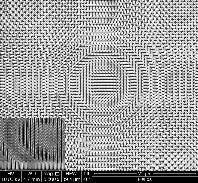
Rotation: the rotation of nanofin structures which creates a Pancharatnam–Berry phase for metalens applications. The metalens pattern is written by electron beam lithography on a GaN epilayer. The pattern has a minimum feature size of 200 nm and minimum distance of 100 nm. Later a layer of Ni metal is deposited as the etching mask by lift-off process. Finally, a ICP/RIE etching process is used to fabricate the high aspect ratio nanofins. A combination of physical etching using Ar as well as chemical etching using cl2 plasma improves the etching rate. The recipe is optimized to obtain maximum aspect ratio and perfect vertical side wall. Image Credit: Oxford Instruments Plasma Technology
The etching was done in Ar plasma with a gas mixture of Cl2/BCl3, which combines the physical etching of Ar plasma and the chemical etching of Cl2/BCl3.
A number of etching parameters must be tuned to ensure the highest etching selectivity and vertical sidewall; for example, ICP power, RF power, Cl2/BCl3 ratio and pressure.
Two key factors must be considered. Ideally, chemical etching should achieve higher selectivity because the metal mask is fairly thin. However, more physical etching is required to achieve the required vertical sidewall. The most ideal recipe strikes a balance between these two processes.
Through ongoing optimization of recipe, it was possible to achieve a selectively of around 30 between Ni and GaN, as well as a good sidewall quality.
Oxford Instruments’ systems played a pivotal role in the development of metalenses. The user-friendly interface of Oxford Instruments’ systems helped to make the processes of sample loading and recipe modification efficient and straightforward, requiring minimal manual intervention.
It was also possible to achieve a good degree of repeatability and uniformity over a large-scale sample surface due to the stability afforded by Oxford Instruments’ systems.
Acknowledgments
Produced from materials originally authored by Ronghui Lin from King Abdullah University of Science and Technology (KAUST).

This information has been sourced, reviewed and adapted from materials provided by Oxford Instruments Plasma Technology.
For more information on this source, please visit Oxford Instruments Plasma Technology.