The majority of metal traces used to produce electrical connections in semiconductor devices begin life as blanket metal films that are later patterned and etched to create conductive connections between elements of a device.
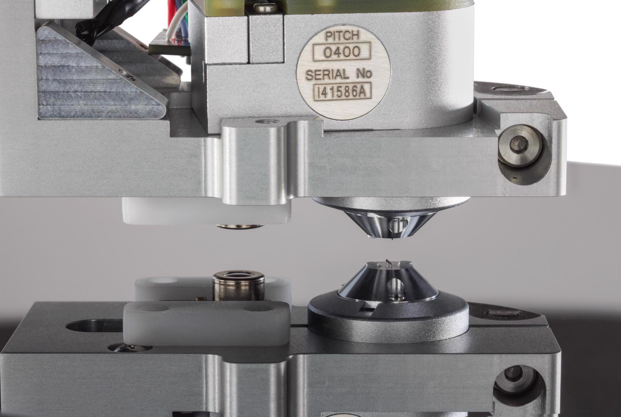
The R50 four-point probe approaches the surface of a conductive layer. Image Credit: KLA Instruments
Wafer uniformity in thin film metal thickness and sheet resistance is vital in order to maximize device performance. This article presents an outline of the KLA Instruments™ Filmetrics® R50 four-point probe and eddy current (EC) techniques for metal film measurement, as well as discussing how to convert the R50 sheet resistance map to a film thickness map.
Four-Point Probe Measurement Technique
The 4PP technique has been in use for over a century, remaining popular due to its accuracy and simplicity. In a four-point probe design, electrical current is transmitted between two pins in contact with a conductive surface while the voltage is measured between two additional pins also in contact with the surface, as can be seen in Figure 1.
Generally, the pin arrangement is either a square or linear array, with this discussion focused on the linear array in use by the R50 probes.
For the bulk of applications, the traditional measurement configuration (Figure 1, left) is used, but an alternate configuration (Figure 1, right) may be used for measurements as part of the R50 Dual Configuration method in cases of current crowding at the edge of a film, or for correction of pin spacing variations. The measurement results detailed here used only the standard configuration.
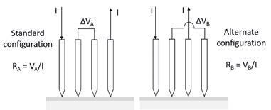
Figure 1. Four-point probe pin schematic for both the standard (left) and alternate (right) linear configurations. The alternate configuration is used as part of the R50 Dual Configuration measurement method, which is typically used in cases of current crowding at the edge of a film or when pin spacing variation requires correction. Image Credit: KLA Instruments
Eddy Current Measurement Technique
The EC technique measures the quantity of eddy current induced in a conductive layer through an applied alternating magnetic field, as exhibited in Figure 2. A time-varying drive current through a coil produces a time-varying primary magnetic field surrounding the coil.
As the probe coil advances towards the conductive surface, time-varying (eddy) currents are induced within the conductive material. These eddy currents generate their own time-varying secondary magnetic field that pairs with the coil, producing a change in signal relative to the sheet resistance of the sample.
The direct results of increased conductivity within the layer are greater induction of eddy currents and greater changes in the real and imaginary impedance of the driving coil.
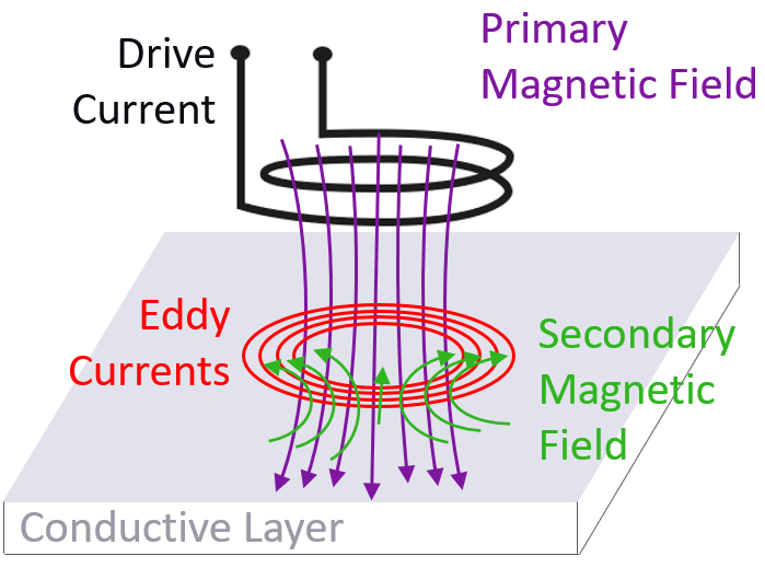
Figure 2. The eddy current (EC) technique generates a time varying current through a coil that creates time varying eddy currents in the conductive layer. These time varying eddy currents in turn create a magnetic field that modifies the impedance of the driving coil, which is inversely proportional to the sheet resistance of the layer. Image Credit: KLA Instruments
R50 Sheet Resistance Data Analysis and Visualization
When 4PP or EC measurements are generated and the sheet resistance (Rs) calculated, the R50 data is managed similarly for each method. Depending on user preference, sheet resistance values can be directly exported, or the data can be changed to film thickness utilizing the conversion feature in the RsMapper software:
Rs = ρ/t
where ρ is the resistivity and t is the film thickness.
The images in Figure 3 display both a sheet resistance map and a film thickness map of a 2 µm nominal thickness aluminum film. From the sheet resistance data (Figure 3, left), a nominal resistivity is used (Figure 3, center) to transform the data into a map of film thickness (Figure 3, right).
Exhibiting the data as a film thickness map can be more suitable and visually meaningful for a number of applications.
The RsMapper software also offers Difference Maps, where the data mapped from two specific wafers are plotted as a single map that displays the differences between them. This feature is of particularly useful for assessing the sheet resistance before and after etching or polishing processes.
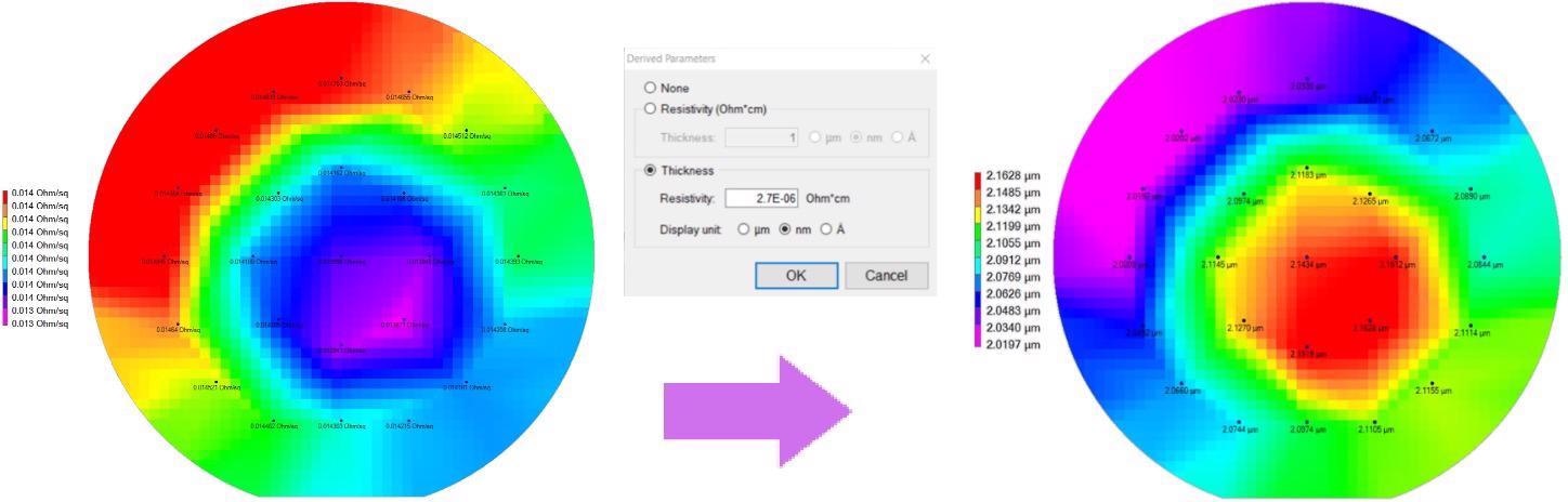
Figure 3. A 2µm thick aluminum layer is mapped for sheet resistance (left). The RsMapper software enables the derivation of film thickness (center) to produce the derived film thickness map (right). The thickness map exhibits an off-center mound, which may be due to an offset in the deposition system. Other possible causes include misalignment of the wafer to the metal target or a slight tilt in the wafer, which will also produce similar patterns. Image Credit: KLA Instruments
Choosing the Appropriate Technique
The maximum sheet resistance of the R50-4PP is 200 MΩ/sq., which makes it perfect for the thinnest of metal films. For extremely thick metal films, the voltage drop (between pins 2 and 3 in Figure 1, left) is rendered as exceptionally small.
In effect this limits the capacity of the 4PP technique to measuring metal films no more than a few microns, depending on the resistivity of the metal.
For sheet resistance measurement, the EC method is restricted to no less than about 100 nm of metal thickness (or about 10 Ω/sq., depending on the type of metal), due to the minimal eddy currents generated by extremely thin metal films.
This limitation is partly a result of the very small spot size of the R50-EC.
In the range where both 4PP and EC techniques can be used, one determining factor may be preventing damage or contamination by way of the pins coming into contact with the sample. The EC technique is recommended for these types of sensitive surfaces.
If the film to be measured is on a conductive substrate that could generate additional eddy currents, the 4PP technique is recommended, on the assumption that an insulation layer is blocking the 4PP DC current.
Other Metal Film Applications
There are a number of applications that necessitate the measurement of buried or backside metal layers. For buried layers, any non-conductive layer impeding contact between the 4PP and conductive layer will invalidate the 4PP technique.
A buried layer can be measured with EC if the resistance of the buried layer is < 10 Ω/sq.
Regarding backside layer applications, this layer can be measured using 4PP if the sample can be positioned face down on the platen. If this arrangement is not possible, the EC technique can usually measure through the face up sample to the distinguish the backside metal layer.
Conclusions
The Filmetrics R50 Series facilitates measurement of a diverse range of metal layers, with the R50-4PP advised for use on thinner films, due to their greater resistance and 4PP’s extensive measurement range.
The R50-EC is recommended for extremely thick films, or for flexible/soft and/or sensitive films where non-contact measurement is needed. The large effective sample clearance also means the R50 can be utilized across a broad range of sample sizes in addition to wafers or thin flat substrates.
For thin film applications, the KLA Instruments group provides addition solutions, such as the Filmetrics family of benchtop and automated tools for measuring film thickness and refractive index.
KLA Instruments nanoindentation systems offer measurement and mapping of film material properties, facilitating characterization of fracture toughness and scratch and wear resistance. Stylus profilers and optical profilers are also on hand for thin film step height measurement.
Image Credit: KLA Instruments
This information has been sourced, reviewed and adapted from materials provided by KLA Instruments™.
For more information on this source, please visit KLA Instruments™.