Researchers using transmission electron microscopes (TEM) continue to stretch the limits of their instruments’ elemental analysis and HR imaging capabilities as they seek to analyze ultra-low damage samples less than 40 nm thick.
When considering appropriate preparation techniques for use with these thin lamellae, it is prudent to consider the class of material being polished and the reproducibility of the method across multiple samples.
This article explores the use of broad argon (Ar) beam ion milling and focused ion beam milling (FIB) – two of the most widely used techniques in the preparation of electron transparent samples for a varied class of materials, including metals, ceramics and semiconductors.
FIB is an especially useful technique where there is a need for specific sample orientation or site-specific positional accuracy. This method can cause a number of issues, however, including implantation, amorphization and vacancies due to the application of high-energy gallium (Ga) ions.
There is also a risk of sample alteration as a result of beam heating or re-deposition, selective abrasion and increased surface roughness.1
FIB-induced surface amorphization is the most extensive and limiting of these issues due to its potential to reduce the signal-to-noise ratio.2
It is also important to avoid geometrical blurring in high-resolution transmission electron microscopy (HRTEM) applications. This requires sample thickness to be reduced by the square root of the feature size.3
It should also be noted that a 25 keV Ga+ FIB column has the potential to generate ~20 nm per sample side damage in silicon (Si)4 – an especially limiting factor in contemporary Si-based semiconductor devices, which often exhibit minimum feature sizes under 20 nm.
The depth of an amorphous layer induced by a FIB is linked to its beam energy, beam angle and the characteristics of the material being milled. There are a number of different techniques suitable for reducing this damage in TEM samples.
- Gas-assisted etching improves the milling rate, but this can also increase the roughness of the crystalline-amorphous interface, impacting the quality of TEM images.5
- Low-energy FIB involves reduced beam energy to help limit the depth of damage. Etching rate and positional resolution are also affected by milling at these energies.
- Wet etching is useful when working with single-layered materials, so long as a suitable solution is used.3 This method cannot be used with multi-layer semiconductor devices due to differences in etching rates, however.
- Argon ion milling represents a promising approach when working with multi-layer materials because it does not feature any of the limitations mentioned here. The initial FIB damage layer is replaced by the newly formed Ar ion-induced damage layer.3,6 This layer’s thickness is dependent on the milling time, energy and angle – parameters which are all user-controlled via the PIPS™ II system.
Practical Aspects of Argon Ion Polishing of FIB Samples in PIPS II
A number of parameters must be considered when looking to optimize new layer thickness formed during Ar polishing of a FIB-induced amorphous layer. This is especially important when it is necessary to avoid re-deposition or sample contamination.
Beam Energy
Low-energy ions offer limited penetration depth, helping to reduce ion-induced surface damage. Beam energies lower than 300 eV are therefore recommended for final polishing steps.
Milling Time
Using the PIPS II system, the Ar ion beam is well focused at low energies (~1 mm FWHM). The current density at the milling area is also high, resulting in a high rate of material removal.
Milling time should therefore be optimized to remove sufficient material to enhance sample quality without over-thinning the sample. It is advisable to mill the sample for a few tens of seconds (<60 seconds) before examining this in the microscope and only milling further where this is necessary.
Milling Angle
A higher beam angle is known to increase ion-induced surface damage, but the low beam energies generally utilized for this application (<0.5 keV) – including the stopping and range of ions in matter (SRIM) models – demonstrate similar sputtering yields at high and low angles.
Higher angles are ideal for post-FIB polishing in the PIPS II system, taking into account constraints imposed by the mounting grid geometry. Milling from both the top and the bottom lowers the chance of thin areas causing the lamella to bend.
Sample Temperature
The stage (sample) temperature should be reduced to ensure that the milling area is kept close to ambient temperature throughout milling. This helps prevent heat-induced damage resulting from ion bombardment.
Ion Milling Mode
The geometry and size of the thin lamellae inside the PIPS chamber mean that it is advantageous to keep the sample stationary, milling this with a single gun at a time. This approach ensures optimum results and minimum re-deposition.
Type of Supporting Grid
Copper (Cu) and molybdenum (Mo) are the two most frequently utilized grid materials. Mo tends to exhibit a lower sputtering rate, reducing the chance of re-deposition from the grid and onto the FIB lamella.
Position of FIB-Thinned Area in Relation to the Milling Gun
FIB samples are typically H-bars or a lift-out type that has been mounted on a grid sidewall or fingertip. After these have been mounted in the DuoPost®, the sample should be placed at the PIPS II Home Position (Figure 1c).

Figure 1. PIPS II optical images of: (a) FIB H-bar sample and (b) FIB lift-out specimen mounted on the side wall of a Cu grid. (c) Top view cartoons show samples in home position as they are inserted in PIPS II system for post FIB polish. Image Credit: Gatan Inc.
The thin lamella should then be brought to the center of rotation using a combination of the PIPS II system’s touch screen alignment page and X, Y stage movement. Orienting the stage rotation angle to allow the ion beam to pass over the lamella prior to milling the substrate or grid will help reduce re-deposition.
When working with lift-out samples mounted on the grid finger’s sidewall, it is necessary to rotate the PIPS II stage around 5º, offsetting this from the pre-set positions available on the alignment page (Figure 2).
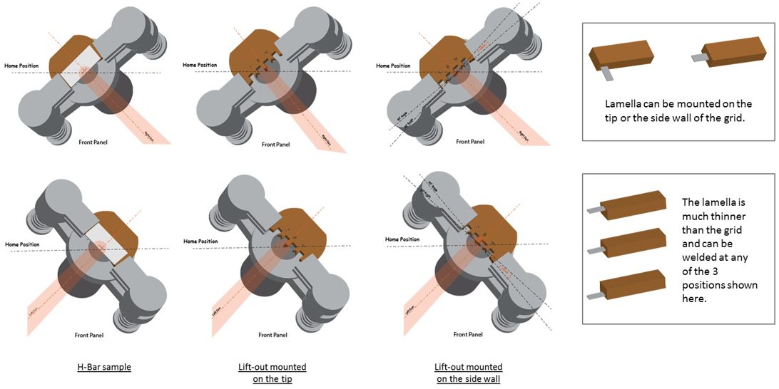
Figure 2. Illustrations show how FIB H-bar and lift-out specimens are oriented with respect to the left and right guns. When lamella is mounted on the side wall of a grid finger, it is better to rotate the specimen at least 5º offset, so the beam does not deposit grid/substrate or weld material on the specimen thin area. Note that as shown in images on the right, the thickness of the lamella is much less than the grid, as a result, the lamella can be welded at different positions on the finger. Image Credit: Gatan Inc.
It should be noted while selecting this offset angle that the Ar beam is approximately 1 mm wide and therefore larger than the lamella.
Results
In the examples presented here, it was possible to improve the quality of FIB-prepared TEM samples – as well as reduce the thickness of the FIB-induced amorphous layer – through the application of low energy (<300 eV), broad beam ion milling using the PIPS II system.
Doing so yielded an overall improvement with no deposition of grid or holder material onto the thin polished area.
Lift-out samples were mounted on either Mo or CuOmniProbe grids, allowing samples to be imaged prior to polishing in the PIPS II System. This afforded the researchers reference of the sample condition following preparation via FIB.
Next, samples were polished using low-energy Ar ion guns in stages, along with sequential observation using a TEM.
The argon beams had been set to mill at incident angles >7° from either the top or bottom, while the lamellae were centered via the PIPS II X, Y stage and aligned to each gun. These were then milled using Stationary Milling Mode. Samples were cooled to -80 ºC during polishing in order to limit heat-induced damage.

Figure 3. Removal of FIB produced amorphous surface layers in a Niobium (Nb) sample can be readily seen in these micrographs. The right image shows changes after 30 s of milling at 300 eV. During this time, the amorphous layer was reduced from approximately 5.6 to 3.5 nm (~40% reduction). FIB prepared specimen provided by University of Chicago, Illinois. Image Credit: Gatan Inc.

Figure 4. TEM micrographs of a multi-layer sample as prepared in FIB (left), after polishing in PIPS II System at 300 eV for 60 s (center), after polishing in PIPS II system for additional 40 s (right). Due to FIB-induced amorphization, the second layer in the middle is not visible in the first two images (left and center), but after sufficient Ar ion polishing, it is clearly visible in the last one (right). FIB prepared specimen provided by Texas Instruments, Dallas Texas. Image Credit: Gatan Inc.

Figure 5. Color images (left) show sample thickness maps* in the device, captured after milling in FIB (H-bar) and low energy milling in PIPS II system (300 eV beam, stationary milling mode, 130 s). Sample thickness is compared in these two images using profile lines averaged along the graph arrows shown below. TEM micrographs (right) show high resolution images taken before and after low energy ion milling in PIPS II system (taken from yellow square areas shown on the thickness maps). By reducing sample thickness, parts of FIB-induced sample surface damage have been removed. FIB prepared specimen provided by Texas Instruments, Dallas Texas. *Rainbow color scale on the thickness maps varies from 0 (black) to 4 (white) mfp. Image Credit: Gatan Inc.

Figure 6. TEM micrographs of a multi-layer sample. The left image was captured as prepared in FIB. The right image was taken after polishing in PIPS II system for 90 s. Due to FIB-induced amorphization, and sample thickness, layers are not clearly visible in the first image, however after Ar ion polishing they are clearly visible. The EELS data (right) shows no sign of re-deposition of grid material (Mo) on the sample. Image Credit: Gatan Inc.
Conclusions
The PIPS II system’s array of novel features includes the ability to leverage focused ion beams at low energies (~1 mm in diameter), stationary milling and custom milling angle capabilities, an easy-to-use X, Y alignment stage, a powerful optical camera and the DigitalMicrograph® imaging software.
These features allow the PIPS II system to efficiently polish FIB samples while maintaining low beam energies <300 eV. This helped improve sample quality while eliminating the risk of holder material (Al) or grid (Mo or CU) re-deposition.
References
- J. Ayache et al in: ”Sample Preparation Handbook for Transmission Electron Microscopy: Methodology”, (Springer, New York) p. 126.
- M.J. Suss, E Mueller and R. Wepf, Ultramicroscopy 111 (2011), p. 1224.
- N.I. Kato, Journal of Electron Microscopy 53 (2004), p. 451.
- L.A. Giannuzzi and F.A. Stevie, Micron, 30, (1999) p. 197.
- K Gamo, Materials Research Society Symposium Proceedings (1993) p. 577.
- A Barna, Journal of Computer Assisted Microscopy, 9, (1997), p. 101.
Acknowledgments
Produced from materials originally authored by Anahita Pakzad from Gatan.

This information has been sourced, reviewed and adapted from materials provided by Gatan Inc.
For more information on this source, please visit Gatan Inc.