Since silicon is the third most abundant element on Earth (after iron and oxygen), it is undoubtedly a readily accessible raw material. It is a significant component of solar cells and electronic devices but must first undergo purification before being used for these purposes.

Image Credit: Shutterstock/Diyana Dimitrova
It is also convenient to separate silicon from ordinary sand by reduction with coke in the presence of iron.
Technical silicon is available in three primary types: amorphous, polycrystalline, and monocrystalline. To achieve metallurgical grade purity, most elemental silicon is first manufactured as a ferrosilicon alloy.
Approximately 15% is further refined to semiconductor purity. Electronic applications require extreme purity at the 99.9999999% level.
The Czochralski technique, in which a seed crystal is suspended in a molten bath of semiconductor-grade silicon and gently drawn while spinning under a protective environment, is often used to create monocrystalline silicon. The outcome is a single, long, spherical crystal ingot that can weigh several hundred pounds.
This crystal is then precision ground for diameter and wire-sawed into discs for extra grinding for flatness and thickness and then polished to specification. Crystal growth technology has advanced to at least a 300-mm diameter and beyond as the semiconductor industry processing benefits from increasingly large-diameter discs.
Although monocrystalline silicon naturally exhibits semi-conductivity, it can be doped with additional elements to produce p-type or n-type silicon. The development of discrete electronic components and integrated circuits is the main application. High-performance photovoltaic components such as solar cells have several uses.
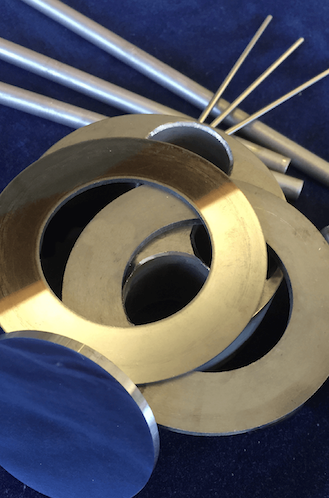
Image Credit: INSACO Inc.-Machining of Hard Materials
Molten silicon is used to cast polycrystalline silicon. Although it does not approach the same levels of purity or electrical efficiency as crystal-grown material, it is nonetheless employed for solar applications since it is less expensive.
Standard silicon wafers are easily accessible commercially and frequently made in-house by semiconductor companies due to years of increasing demand for precision wafer fabrication. Wafers are made using highly automated techniques, making them extremely affordable.
Since 1947, INSACO has acquired the knowledge and tools necessary to precisely measure and shape various technical ceramics. INSACO purchases single crystal silicon in larger sizes with the appropriate specifications, and it accurately fabricates distinctive characteristics to the users’ designs.
Specific R&D initiatives for the National Laboratories have benefited from this.
Source: INSACO Inc.-Machining of Hard Materials
| Property |
Value |
| Mechanical |
| Density |
2.33 gm/cc |
| Hardness |
1150 Knoop |
| Tensile Strength |
16.4 kpsi |
| Modulus Of Elasticity |
18.8 - 27.3 x 10⁶ psi |
| Flexural Strength |
43.5 kpsi |
| Poissons Ratio |
0.28 |
| Fracture Toughness |
3 - 6 MPa m1/2 |
| Electrical |
| Dielectric Constant |
11.8 (@ 1 MHz) |
| Volume Resistivity |
10-3 ohm-cm |
| Thermal |
| Coefficient Of Thermal Expansion |
2.6 x 10⁻⁶/°C |
| Thermal Conductivity |
156 W/mK |
| Specific Heat |
0.15 cal/g °C |
| Maximum Working Temperature |
1350 °C |
| Optical |
| Index Of Refraction |
1.54 |
| Transmission Band |
0.30 - 37 Wavelength (microns) In the IR Range |
All properties are at room temperature unless otherwise noted.
Engineering data are representative, and are not intended as absolute nor warrantable. Manufacturer’s Data shown is blended from multiple sources and therefore illustrates the marketplace.

This information has been sourced, reviewed and adapted from materials provided by INSACO Inc. - Machining of Hard Materials.
For more information on this source, please visit INSACO Inc. - Machining of Hard Materials.