In this interview, AZoM talks to Geoff Downing and Mark Mattison from Thermo Fisher Scientific and Entegris, respectively, about semiconductors and their importance, manufacture and how gas analysis factors into these processes.
Where Are Semiconductors Used? Powering Everyday Life and Modern Technology
Video Credit: Thermo Fisher Scientific
Could you please introduce yourselves and tell us a little about your background?
Geoff Downing:
I am Geoff Downing, an industry insider and a Business Development Manager from Thermo Fisher Scientific.
Mark Mattison:
I am Mark Mattison. I am a Quality Assurance Lab Supervisor from Entegris and an analytical chemist by trade.
What makes you an industry insider, Geoff?
Geoff Downing:
I am an advisory committee member for the Global Automotive Advisory Council for SEMI, an advocacy group. I am also a member of the Smart Manufacturing Global Executive Committee. These roles mean I am well-informed about the latest trends and challenges within the industry.
How important are semiconductors to everyday life and how have they evolved?
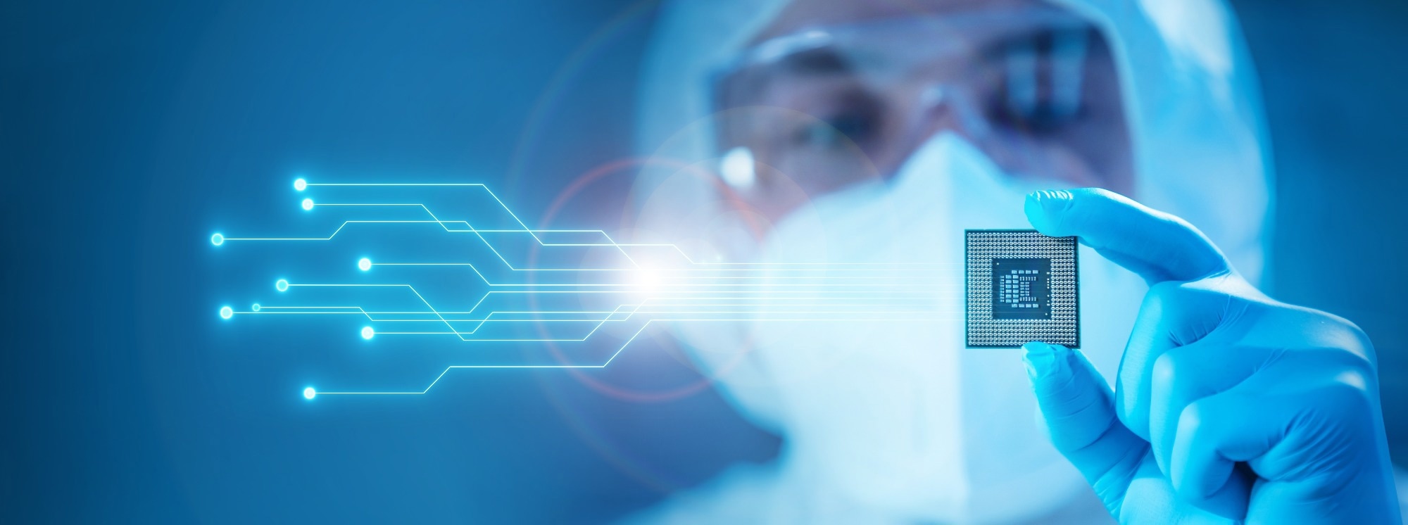
Image Credit: Maksim Shmeljov/Shutterstock.com
Geoff Downing:
Semiconductors are silicon chips that conduct electricity. They are very important for everyday life as electronic devices, such as cell phones, televisions, and medical equipment, rely on semiconductors.
There is an ongoing movement regarding the Internet of Things. While you may not care about a smart spatula with the latest and greatest semiconductor chip, you care if your pacemaker or car with early collision technology has this.
This has been the progress made with Moore's Law in the semiconductor industry. While we have moved beyond more is more, we are still moving into other areas and getting down to the smallest technological nodes. The industry is pushing the limits of current manufacturing capabilities.
For example, the wiring on a semiconductor chip is currently 500 times smaller than a human hair. We manufacture at the smallest scale possible, smaller than bacteria and viruses.
What is Moore's Law?
Geoff Downing:
The basis of Moore's Law is that the number of transistors on a chip doubles every two years. This has been the momentum behind the increases in technology, but there have been other trends within the industry to help propel this.
Cars are manufactured at the 25-30 nanometer scale, while cutting-edge computer chips are manufactured at seven nanometers, perhaps even five. We are pushing beyond this and looking at R&D to manufacture at the scale of two or three-nanometer chips.
What is driving growth in demand, and which industries are asking for semiconductors?
Geoff Downing:
Automotive is a critical driver in the industry. Over 50% of the total cost of automotives is due to the semiconductor chip technology within it. Moving from combustion engines to battery-powered cars means semiconductor chips will entirely control them.
The onboard systems on these cars must have cutting-edge imagery detection technology, battery management systems, and applications. This is only going to improve and grow.
Another primary driver of the industry is AI and cutting-edge computers. Supercomputers will tackle some of the most significant issues facing humanity, and the latest semiconductor technology will power them.

Image Credit: Fahroni/Shutterstock.com
Semiconductors are small but important as they drive modern life, but how are they made?
Geoff Downing:
Semiconductor chips go through a very long manufacturing process, taking between 120 days and nine months, depending on the type of chip and supply chain involved. These are global supply chains supporting the completed product.
Semiconductor chips could be manufactured primarily in-house by a large fabrication plant, but there are also diversified approaches, where the chip moves across countries to complete certain stages of its manufacture.
Generally, there are three phases to any manufacturing semiconductor chip. Firstly, design is primarily dominated by the US, with over 50% of the market. Following this is front-end manufacturing within the extensive facilities and fabs. Lastly, there is a backend considered as packaging.
Some companies design chips but do not necessarily make them. Could you tell us a bit more about this?
Geoff Downing:
There are some large names in the semiconductor industry that outsource the manufacturing front end. This is generally because it involves clean room work, which needs to be done in one location. This means you cannot send the product across until a critical step is completed in the manufacturing process.
There are usually over 150 different steps within manufacturing a semiconductor chip and it cannot be exposed to the atmosphere. Special wafer movement systems within these fabs carry it across floors and chambers to protect it from the local atmosphere.
The environment of the semiconductor fab is so well controlled that it is 500 times cleaner than a surgical operating room.
What could happen if impurities are introduced into the process?
Geoff Downing:
Failure of the chip is likely if impurities interact with the wafer or the dyes during the manufacturing process.
If a dust molecule were to land on any of these chips, the molecule's whip is wide enough to block the passage of electrical current on the chip, making the chip ineffective and inoperable.
Could you describe a few examples of the chemicals and gases introduced during the manufacturing process of a semiconductor?
Geoff Downing:
Manufacturing of semiconductors uses a wide range of gases, but helium, nitrogen, argon, and hydrogen are most widely used across all these processes.
What is your role in your laboratory, Mark?
Mark Mattison:
My role is to monitor the purity of the gas we use at our factory. The gases used in the industry are to create or promote the chemical reactions required to shape the electrical properties of the semiconductor chip.
Nitrogen is a prevalent gas in the semiconductor industry, often used to purge and clean the chip surface. A single molecule of dust can completely obliterate the entire chip, costing millions of dollars and lots of resources.
To purge your semiconductor chip with nitrogen, you must ensure it is clean. If your nitrogen contains oxygen or carbon monoxide, it will cause problems. Materials must be pure in semiconductor manufacturing.
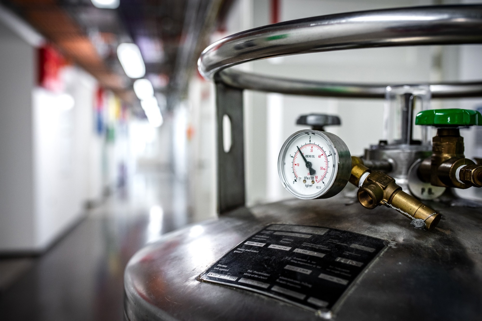
Image Credit: Forance/Shutterstock.com
How do you measure the tiny amounts of impurities, and is there a certain technology that you prefer?
Mark Mattison:
My experience is mostly with mass spectrometry, one of the best ways to analyze such compounds. Specifically, we use an APIMS, an atmospheric pressure ionization mass spectrometer, simplifying the analysis of big bulk gases.
Around 20 to 30 years ago, you could not achieve very low detection limits when analyzing oxygen in bulk nitrogen, but Thermo Fisher Scientific offers analyzers with a low detection limit. This allows us to accurately say we will get 10 to 15 parts per trillion in our gases used in these processes, which is almost an unfathomable number.
This is where the technology has evolved. We can now ionize the bulk gases, charge the bulk nitrogen, and ionize it to bump into the tiny impurities and start ionizing them. This is a much more efficient way to measure such small levels in bulk gas.
Is the industry demanding more purity from the gases and chemicals that they are using?
Geoff Downing:
Yes, the industry is getting increasingly sophisticated. It is being driven through capabilities that are always expanding. As they expand, the manufacturing demands also narrow their process windows.
The manufacturing process that was acceptable five or 10 years ago is not fathomable to use to manufacture the next generation of chips. The process needs to become more specific, with increasing control over the environment in the atmosphere to generate these technological advances.
Any residual gas left within the chamber reacts and interferes with any chips on the wafer. In each of these processes, multiple gas recipes are used. For example, nitrogen purges the previous gas recipe out of the chamber entirely. Then, a new gas chamber process begins with a unique cocktail of gases to enhance the chip’s capabilities and material properties.
If any of these processes go wrong, all the materials and man-hours spent on that chip are lost. The cost of scrap within these manufacturing steps is very quickly astronomical. To mitigate those losses through scrap and to enhance the yield within these manufacturing sites, they must continually narrow their specifications.
This is why fabs cannot reuse the facilities and old equipment. They must continually purchase the latest and greatest to push the boundaries of their R&D and, in turn, push the latest production lines that will lead the future.

 Check out the 'Science With a Twist' podcast!
About the interviewees
Geoff Downing
Business development manager at Thermo Fisher Scientific
Noteworthy: Geoff is active in key semiconductor advocacy groups and organizations, influencing the semiconductor industry value chain and advocating for government support. He's part of the Global Automotive Advisory Council (GAAC), Smart Manufacturing Global Executive Committee (GEC), and steering committee.
Where to find him: LinkedIn

Mark Mattison
Quality assurance lab supervisor at Entegris
Noteworthy: Mark is an analytical chemist by trade and has worked as a Lab Supervisor over the past few years.
Where to find him: LinkedIn


This information has been sourced, reviewed and adapted from materials provided by Thermo Fisher Scientific – Environmental and Process Monitoring Instruments.
For more information on this source, please visit Thermo Fisher Scientific – Environmental and Process Monitoring Instruments.
Disclaimer: The views expressed here are those of the interviewee and do not necessarily represent the views of AZoM.com Limited (T/A) AZoNetwork, the owner and operator of this website. This disclaimer forms part of the Terms and Conditions of use of this website.