Nanoindentation is a non-destructive technique employed to the determination of the micromechanical properties of various materials. The main mechanical properties that are determined with this method is the hardness and modulus of elasticity, often referred as Young's modulus. These properties are derived from the obtained load curves during the interaction between the indenter tip and the sample material. The load curves encompass two main physical quantities, which are continuously measured: the applied load force and the penetration depth.
An interesting application field involves the determination of fracture toughness in the measured samples. The analysis of the residual imprint, along with the mechanical parameters and applied force, are proportional to the value of the fracture toughness. Nanoindentation testing for this purpose can be conducted using the Semilab IND-1000 or IND-1500 equipment.
Application Areas
- Raw material manufacturers
- Thin film coatings
- Failure analysis
- Quality control
- Evaluation of brittle materials
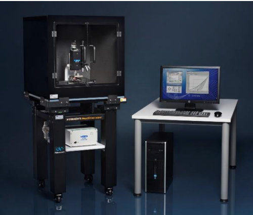
Figure 1. IND-1500 system. Image Credit: Semilab Semiconductor Physics Laboratory
Metrology
During a nanoindentation measurement, the position, i.e., the penetration depth of the tip on the loading head, is being measured alongside the applied loading force. The tip is typically made of hard materials, often diamond, with a specialized geometry. After precise calibration, users can calculate the hardness and modulus of elasticity of the samples based on the obtained loading and unloading curves.
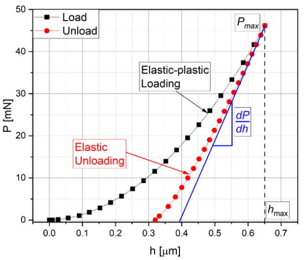
Figure 2. Load-Displacement curve. Image Credit: Semilab Semiconductor Physics Laboratory
The hardness is determined by the ratio of the maximum applied load force to the contact area, giving it a dimension of N/m2 = Pa. The modulus of elasticity is proportional to the initial slope of the unloading curve, which corresponds to the expansion of the material under decreasing mechanical stress.
Another application of indentation testing, though less commonly known, involves the determination of fracture toughness. This process relies on visualizing the crack size and may necessitate the use of an optical microscope or an Atomic Force Microscope (AFM), depending on the size of the imprint and the crack. Cracks typically manifest at the corners of the residual impression in brittle materials.
Use Case
A substantial amount of stress is applied to the specimen material using a Cube Corner indenter tip. This method is considered non-destructive as it does not lead to specimen fracture.
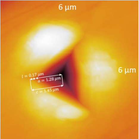
Figure 3. AFM image of indentation made in copper using a cube corner indenter. Image Credit: Semilab Semiconductor Physics Laboratory
The following formula represents one of the calculation approach for determining fracture toughness:
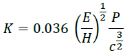 ,
,
where K stands for the fracture toughness of the sample, E is the modulus of elasticity of the sample, H is the hardness of the sample, P denotes the maximum applied loading force and c is the length of the appearing crack.
Materials and Structures
In nanoindentation, sample size is restricted. For IND-1000 and IND-1500 configurations, the maximum height is 15 mm, with a maximum diameter of 50 mm. Ideally, hard materials such as glass, ceramics, hard composites, and metals are suitable for testing. These samples do not require special handling.
This procedure offers certain advantages over more conventional methods, as it can be performed on the surface of materials without requiring extensive specimen preparation or the introduction of pre-existing cracks or notches. This method is especially well-suited for brittle materials.
References and Further Reading
- Nguyen Q. Chinh et al. Extended Applications of the Depth-Sensing Indentation Method [2020], https://www.mdpi.com/2072-666X/11/11/1023
- Anthony C. Fischer-Cripps: Nanoindentation (Third Edition), DOI: 10.1007/978-1-4419-9872-9

This information has been sourced, reviewed and adapted from materials provided by Semilab Semiconductor Physics Laboratory.
For more information on this source, please visit Semilab Semiconductor Physics Laboratory.