First, can you tell us a bit about yourself and your role at Bruker?
As the Product Manager EBSD in the Electron Microscope Analyzers Business Unit in Bruker Berlin, Germany, I am responsible for defining the EBSD product roadmap. I am also deeply involved in various R&D projects with internal and external teams. I represent Germany as an EBSD expert in the ISO committee and work on various EBSD-related projects.
I am a metallurgical engineer with a PhD in severe plastic deformation of FCC metals. I have been using EBSD since 2003, first in academia and research environments and later in the industrial environment. I have authored/co-authored multiple peer-reviewed papers and patents focused on EBSD-related methods and solutions.
The eWARP detector represents a significant step forward in EBSD technology. What were the primary goals or challenges that drove its development?
The development of eWARP was driven by a clear vision: to redefine the limits of EBSD performance in terms of speed, sensitivity, and spatial resolution. Our primary goals were to enable ultra-fast data acquisition, high-fidelity pattern capture, and robust performance on applications, e.g. heavily deformed, ultra-fine grained and beam sensitive materials.
One of the biggest challenges was balancing speed with signal efficiency or sensitivity - ensuring that even at warp-speed acquisition rates, the quality of crystallographic data remains uncompromised and beam requirements remain moderate.
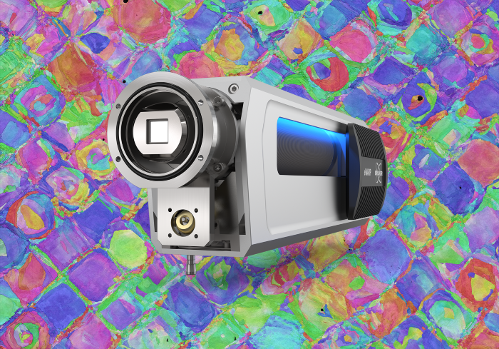
eWARP, the fastest and most sensitive EBSD detector ever, on a background of a 3D printed steel sample with resolved features as small as 100 nm wide. Image Credit: Bruker Nano GmbH – Electron Microscope Analyzers
eWARP is noted for its advanced optics and high-speed data acquisition capabilities. Can you explain how these features translate into practical advantages for researchers and microscopists?
Absolutely.
EBSD is entering a new era of speed and precision. This leap in performance unlocks applications that were once out of reach: automated 3D EBSD acquisition can now be completed faster, at higher pixel resolution, or across larger volumes; ultra-fine grained and heavily deformed materials benefit from spatial resolution down to 20 nm without sacrificing speed; and even time-resolved EBSD mapping, i.e. capturing repetitive maps every few seconds, becomes feasible, enabling real-time insights into microstructural changes during in-situ heating or mechanical testing.
Integration and user experience are often critical in analytical instrumentation. What has Bruker done to ensure the eWARP system is both accessible and adaptable to a range of SEM platforms and user needs?
eWARP is compatible with most SEM platforms, including both new and legacy systems. The eWARP detector is supported by Bruker’s intuitive software suite, which offers automated calibration, real-time feedback, and a a wide range of tools for data post-processing and visualization. Whether you're a seasoned electron microscopist or a new user, the system is designed to be accessible, flexible, and scalable - from routine EBSD to advanced correlative techniques like combined EDS & EBSD.
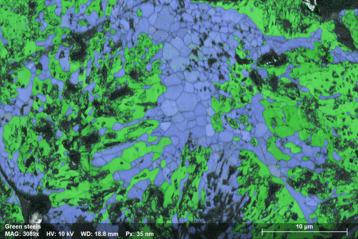
Phase map showing the distribution of Magnetite (blue) and Ferrite (green) in a Hematite pellet sample following hydrogen reduction for 20 minutes. eWARP was used to study the microstructural evolution of this sample over the reduction process. Learn more about this application.
Image Credit: Bruker Nano GmbH – Electron Microscope Analyzers
With your background in nanostructured materials and microanalysis, how do you see eWARP influencing future research directions in materials characterization?
By making low-kV EBSD the new norm, eWARP opens exciting possibilities in nanostructure analysis, especially in fields like energy materials, semiconductors, and advanced alloys. Its speed and sensitivity make it ideal for characterizing fine-grained structures, interfaces, and defect distributions at unprecedented spatial resolution. I’m confident that eWARP will redefine the landscape of materials research by empowering scientists to transition a significant portion of their work from TEMs to SEMs. This shift leverages the far greater accessibility of SEMs, unlocking unprecedented throughput and accelerating discoveries at a pace that will transform both technological innovation and scientific progress.
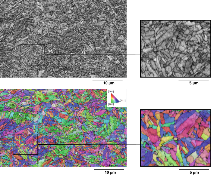
EBSD results acquired from a martensitic steel sample measured at 10 kV and 12 nA. Such structures are notoriously difficult to accurately map at high resolution using a conventional EBSD detector. Learn more about this application.
Image Credit: Bruker Nano GmbH – Electron Microscope Analyzers
In your role as Product Manager, how do you gather and incorporate feedback from the scientific community to guide ongoing improvements or updates to the eWARP system?
We maintain close relationships with our user community through technical workshops, beta testing programs, and collaborative research projects. Feedback is gathered continuously; from performance metrics to usability suggestions and fed directly into our development pipeline. We also monitor emerging trends in academic literature and industrial applications to anticipate future needs. This iterative approach ensures that eWARP evolves in step with the scientific frontier.
Looking ahead, what technological trends or user demands do you foresee shaping the next generation of EBSD systems beyond eWARP?
I see a strong push toward multi-modal analysis, where EBSD is integrated seamlessly with techniques like EDS, and even machine learning-based analysis. There’s also growing interest in automated, AI-assisted workflows that reduce user intervention and improve reproducibility. Future EBSD systems will likely offer higher spatial resolution, higher productivity, better data quality and angular resolution and cloud-based data management, enabling collaborative and remote research environments.
Finally, what excites you most about working on cutting-edge tools like eWARP, and how do you see your work contributing to the broader mission of Bruker in advancing materials analysis?
What excites me most is the opportunity to empower researchers and engineers with tools that push the boundaries of what’s possible. eWARP is not just a detector, it’s a platform for discovery.
Being part of a team that translates scientific challenges into technological solutions is incredibly rewarding. At Bruker, our mission is to advance materials analysis through innovation, and I’m proud to contribute to that by helping engineers and scientists unlock new insights into the structure and behavior of materials.
About Daniel Goran
Daniel Goran is a Senior Product Manager for Electron Backscatter Diffraction (EBSD) at Bruker Nano GmbH, where he has spent more than 13 years driving the growth, competitiveness, and technical direction of the EBSD product portfolio.
With a background that spans application science and product management, Daniel combines deep technical expertise with a strong understanding of market needs to support advanced materials characterization workflows. He previously held roles as an EBSD Application Scientist at Bruker Nano and Oxford Instruments HKL, working closely with researchers and engineers to optimize SEM-based microstructural analysis.
Daniel holds a PhD in Materials Science from Paul Verlaine University Metz, as well as master’s degrees in Physics and Metallurgy. His expertise includes materials science, scanning electron microscopy, and crystallographic characterization, and he is based in Berlin, Germany.
This information has been sourced, reviewed, and adapted from materials provided by Bruker Nano GmbH – Electron Microscope Analyzers.
For more information on this source, please visit Bruker Nano GmbH – Electron Microscope Analyzers.
Disclaimer: The views expressed here are those of the interviewee and do not necessarily represent the views of AZoM.com Limited (T/A) AZoNetwork, the owner and operator of this website. This disclaimer forms part of the Terms and Conditions of use of this website.