Within materials science, the surface is often where the most important interactions occur. Whether the focus is corrosion, catalysis, adhesion, or biomaterials, the outermost atomic layers determine performance and durability.
X-ray photoelectron spectroscopy (XPS) imaging is a reliable methodology for visualizing and quantifying surface chemistry with spatial resolution. By integrating elemental analysis with imaging capabilities, XPS provides a distinct perspective on the chemical composition of materials at the nanoscale.
This article examines the capabilities of various XPS imaging modes, ranging from macro-scale mapping across millimeter ranges to parallel, astigmatic XPS imaging with micron-level spatial resolution. It emphasizes how these techniques are vital for moving beyond the premise of surface homogeneity.
The Flawed Premise: Why Conventional XPS May be Insufficient
Traditional XPS and related methodologies, such as hard X-ray photoelectron spectroscopy (HAXPES), offer elemental composition and thickness calculations; however, they fundamentally rely on discrete sampling points and presuppose uniform surface coverage.
In the rigorous domain of materials science, this assumption can represent a significant vulnerability. In spectroscopy mode, the spectrum is obtained from an area defined by either a lens or an X-ray probe. The resulting spectrum is an average derived from the entire area from which photoelectrons are gathered.
For many samples, elemental or chemical variations may exist on a scale smaller than the analyzed region. Conversely, differences might occur on a much larger scale. In such instances, the generation of laterally resolved maps or images of the distribution provides essential data.
Revealing Millimeter-Scale Inhomogeneity
Contemporary XPS instrumentation can define a series of analysis positions that correspond to specific XY stage coordinates across a sample.
The collection of a survey spectrum at every position enables the creation of an elemental relative-concentration map, in which a heat map indicates the concentration of elements within the uppermost atomic layers.
This is demonstrated by the coverage of a self-assembled monolayer (SAM) polymer adsorbed onto gold. It's immediately evident that, despite the assumption that the SAM is uniform, an area exists where the gold substrate signal is significantly more intense.
This brighter region coincides with a reduction in carbon, oxygen, and nitrogen associated with the SAM polymer. These maps reveal millimeter-scale inhomogeneity in the material's coverage.
Here, the primary advantage is strategic in nature: macro-scale mapping provides proof regarding whether a sample is homogeneous or not before time and resources are expended on detailed, yet ultimately non-representative, high-resolution analysis.
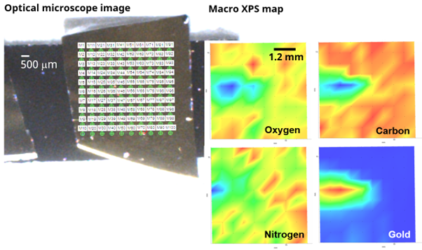
Image Credit: Kratos Analytical, Ltd.
High Spatial Resolution XPS Imaging: Two Methodologies
While macro-scale mapping offers quantitative distribution over a millimeter scale, a requirement often exists to understand chemical distribution at a much higher spatial resolution. There are two distinct strategies for high spatial resolution XPS imaging, differentiated as XPS mapping and astigmatic or parallel XPS imaging.
XPS mapping utilizes a focused X-ray beam that is scanned across the sample in a point-by-point fashion, sequentially gathering narrow energy region spectra from the surface. In XPS mapping, the final spatial resolution is determined by the diameter of the X-ray spot.
In contrast, parallel XPS imaging records a full-field image simultaneously by using energy-filtered electron optics and an astigmatic lens system.
This methodology is comparable to light microscopy, in which a surface image is magnified and projected onto a two-dimensional detector. Parallel XPS imaging is generally faster and offers superior ultimate spatial resolution compared to XPS mapping.
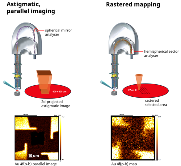
Schematic diagram showing parallel imaging using the AXIS spherical mirror analyzer (left) and mapping using the hemispherical sector analyzer. Also shown are the Au 4f peak minus background images acquired using parallel imaging and mapping respectively. Image Credit: Kratos Analytical, Ltd.
Expanding Data Derived from XPS Imaging
Selected Area XPS
The advantages of determining the lateral distribution of elemental and chemical components at the surface have been established. Additional valuable data can be extracted from a sample by utilizing an image to identify a region of interest for spectral analysis.
Selected area XPS is a useful mode of spectral acquisition in which either the probe size is decreased or an aperture is placed into the lens to define the specific area from which photoelectrons are collected.
This type of acquisition allows for spectral acquisition from a precise area of interest, such as a defect, an inclusion, or a patterned feature. The capability makes the technique ideal for heterogeneous materials, microelectronic devices, and failure analysis, where spatially resolved chemical information is vital.
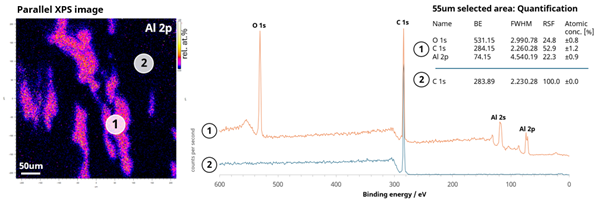
Aluminum distribution revealed by XPS imaging of a delaminated multi-layer potato chip packaging material. 55 μm diameter selected area spectra were taken from 2 discrete analysis positions defined from the Al 2p 400 x 400 μm parallel XPS image. The materials were identified as corresponding to the polypropylene inner layer and (oxidized) aluminum barrier layer. Image Credit: Kratos Analytical, Ltd.
Stitched XPS Imaging
To continue the comparison of light microscopes, parallel imaging features fixed fields of view defined by specific lens settings. Every magnification level has a corresponding spatial resolution. Some samples will certainly necessitate high spatial resolution XPS imaging over regions larger than the lowest possible magnification allows.
In these instances, it is possible to employ stitched imaging, where parallel XPS images are obtained as a function of stage position, with the stage moving in exact multiples of the field of view. The benefit of this type of imaging is the acquisition of high spatial resolution images spanning several millimeters.
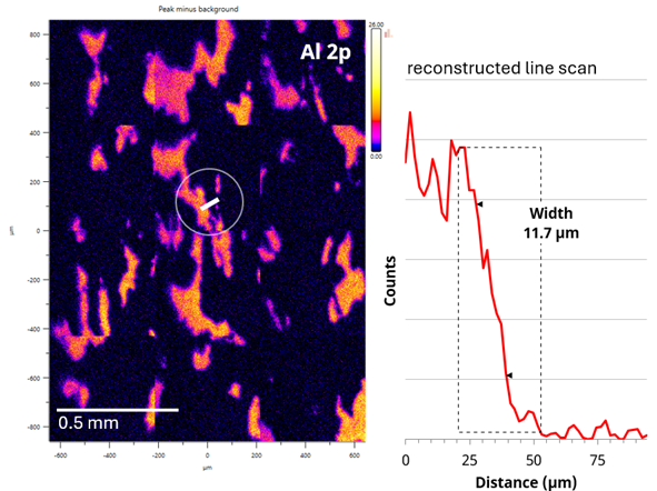
A 3x4 stitched parallel image of Al distribution over a 1.3 (w) x 1.9 (h) millimeter area of the delaminated multilayer food packaging material. The linescan generated from this image shows an edge resolution of ∼12 μm. Image Credit: Kratos Analytical, Ltd.
Spectromicroscopy: Spectrum at a Pixel
The discussion thus far has concentrated on the spatial resolution of the image, but an interesting topic exists regarding energy resolution.
Just as with spectroscopic acquisition, XPS images can be obtained at various energy resolutions, typically depending on whether the requirement is for elemental (low energy resolution) or chemical state (higher energy resolution) images.
A sophisticated acquisition mode of the AXIS generation of XPS instruments is spectromicroscopy, also known as "spectrum at a pixel." This acquisition mode involves the recording of a series of parallel images as a function of energy, moving through the specific energy range of interest.
Once the collection is finished, the dataset contains a spectrum for every pixel in the image. Although the total acquisition time for this type of experiment may reach several hours, the presence of more than 65,500 pixels per image means the effective acquisition time per spectrum is approximately 165 milliseconds.
The signal-to-noise ratio of an individual spectrum will be quite low. However, such extensive datasets are appropriate for multivariate analysis, which permits principal component analysis and the extraction of meaningful "spectrum at a pixel" data with an energy resolution sufficient to identify chemical shifts.
Further software capabilities allow these spectra to undergo background subtraction and curve fitting with multiple components. Subsequently, images are reconstructed to display the lateral distribution of every chemical component. Spectromicroscopy mode is remarkably powerful, making it possible to obtain chemically resolved spectra from an area smaller than 2 x 2 μm.
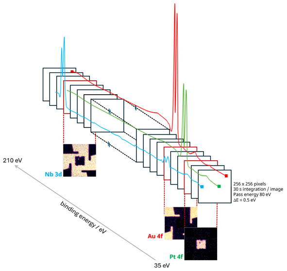
Schematic of spectra from image dataset. Thirty-second images were acquired at 0.5 eV energy intervals between 210 – 35 eV binding energy. Images corresponding to Pt 4f, Au 4f, and Nd 3d peak maxima are shown. Acquiring data at 80 eV pass energy gives good energy resolution and sensitivity. Image Credit: Kratos Analytical, Ltd.
Imaging as the Analytical GPS
This brief summary demonstrates that the true utility of XPS imaging is achieved when it serves as an "analytical GPS", directing subsequent and more detailed spectroscopic analysis. XPS imaging enables materials characterization ranging from macro-scale mapping of inhomogeneity to precise, micro-scale spectromicroscopy.
Guiding Surface Analysis into a Spatial Domain
The integration of sophisticated XPS imaging modes – from macro-scale mapping for quantitative spatial distribution to high-resolution XPS image stitching for defect detection – continues to revolutionize surface characterization.
For researchers developing devices, coatings, or biocomposites, XPS imaging ensures that performance metrics are established based on verifiable, spatially consistent chemical compositions rather than on averaged or assumed information.
XPS imaging is a vital step in contemporary surface science, transitioning the field from the collection of a few isolated data points to the surveying of the entire chemical landscape.
By offering a high-resolution perspective on surface chemistry, the necessary context is gained to predict material behavior, diagnose failure, and design superior products. Kratos Analytical, using over 50 years of expertise, continues to drive this development, ensuring these advanced capabilities, including unmatched automation, are available to laboratories globally.

This information has been sourced, reviewed, and adapted from materials provided by Kratos Analytical, Ltd.
For more information on this source, please visit Kratos Analytical, Ltd.