As electronic waste climbs, researchers say the branching architecture of ordinary leaves could help create transparent electrodes and compostable circuit substrates with a fraction of the carbon footprint.
 Study: Leaftronics: Bio-Fractal Scaffolds From Leaf Venation for Low-Waste Electronics. Image Credit: Yulcha/Shutterstock.com
Saving this for later? Download a PDF here.
Electronic waste is ever-increasing, driven in part by materials built to last in use - but not to break down at end of life. Printed circuit boards and flexible electronics rely heavily on non-degradable materials that are difficult to recycle and often end up in landfill. Transparent conductors such as indium tin oxide also remain widely used despite material scarcity, high processing energy, and mechanical brittleness.
That leaves the field with a materials dilemma. Electronic platforms increasingly need optical transparency, smooth surfaces for thin-film deposition, thermal stability for soldering, and end-of-life degradability in the same system. Existing options usually improve one of those properties at the expense of another.
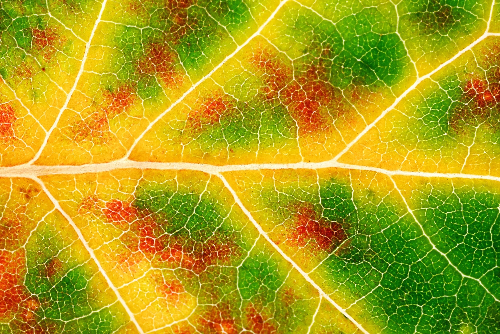
This Perspective in Advanced Materials presents Leaftronics as a possible option. The concept behind this is to use the quasi-fractal venation networks found in leaves as lignocellulosic scaffolds for electronic materials. Those naturally evolved structures combine efficient transport, mechanical support, and low material use.
Practically, the scaffold can then be paired with biodegradable polymers or conductive coatings to create decomposable substrates and transparent electrodes.
Creating Leaf-Based Electronic Scaffolds
The process is designed to preserve the leaf’s natural hierarchy. Leaves are treated in an alkaline solution to remove soft tissue and pigments, leaving behind a lignocellulosic skeleton. The remaining scaffold retains a quasi-fractal vein network with micrometer-scale features. Cleaning and surface-activation steps improve adhesion and prepare the structure for further integration.
From there, the platform branches in two directions. In one route, conductive coatings such as silver nanowires or silver microparticle inks are applied to the venation network to form transparent electrodes. In the other, the scaffold is infiltrated with biodegradable polymers, including ethyl cellulose or gelatin, to form composite substrates with smooth surfaces and good mechanical stability.
Key to the paper is that this scaffold-preparation route is relatively simple and low-energy compared with approaches such as nanocellulose processing. At the same time, the resulting materials are meant to fit into established electronics workflows, including vapor deposition, printing methods, and reflow soldering.
What Performance The Platform Can Deliver
The study reviews prior results on both substrate and electrode performance. For substrates, polymer-infiltrated leaf structures have been reported to deliver surface roughness below 1 nm, optical transmittance above 85 %, and enough thermal stability to tolerate reflow soldering. The paper also describes their use in thin-film devices, printed electronics, and circuit integration while maintaining flexibility and structural integrity.
For electrodes, metallized leaf venation networks can reach low sheet resistance, in some cases below 1 Ω/sq, while retaining high optical transparency. The value of the architecture lies in its hierarchy: the branching network can support charge transport while using relatively little conductive material.
When comparing synthetic and biomimetic fractal electrodes, natural leaf-derived networks show comparable performance and, in some cases, better.
The authors stress that structure matters. Vein density, branching hierarchy, and fractal dimension all influence electrical percolation, optical haze, and mechanical behaviour. So performance is not just about the coating or polymer used, but also about selecting and tuning the biological feedstock itself.
Why Sustainability is a Central Consideration
The environmental argument is one of the paper’s main themes. The authors discuss a preliminary, non-ISO-compliant life-cycle analysis indicating that Leaftronic substrates could have a much lower carbon footprint than conventional materials such as FR4 and PET.
The platform also supports end-of-life recovery: electronic components can be separated through mild chemical or enzymatic processing rather than being trapped in conventional board materials.
The biodegradability claim is also more specific than it may first appear.
The paper points in particular to ethyl-cellulose-based substrates, which showed rapid degradation under defined composting or related breakdown conditions, including industrial composting environments. That is an important nuance because the Perspective does not suggest that every Leaftronics variant will behave identically under all disposal conditions.
Where Solutions are Still Sought
The paper is careful not to present Leaftronics as a finished answer. It highlights several technical challenges, including humidity-related adhesion issues, variability from leaf to leaf, thermal limits in biodegradable polymer matrices, and the need to control silver-ion release in some electrode systems.
It also makes clear that Leaftronics is not being pitched as a near-term replacement for high-performance silicon microelectronics. The approach is instead framed as a complementary strategy: one that could reduce waste tied to substrates and interconnect materials while still allowing recovery of valuable components.
Much of the mass in electronic waste comes from the materials used to hold and connect chips. If those structural materials can be made lower-carbon, degradable, and easier to disassemble, that could improve the sustainability of electronics without requiring an immediate rewrite of semiconductor technology.
Next Steps for Leaftronics
The next steps are practical as well as scientific. The authors point to the need for better control over structure-property relationships, better management of natural-feedstock variability, and a wider set of biodegradable polymers and conductive coatings. They also highlight data-driven approaches, including machine learning and materials informatics, as tools for choosing leaf types, refining processing conditions, and matching scaffold structures to particular device needs.
Overall, the Perspective argues that natural leaf venation is more than a visual inspiration. It could offer a ready-made hierarchical template for electronic materials that are lighter on resources, easier to recover, and more compatible with circular manufacturing.
Journal Reference
Rajendran, R. et al. (2026). Leaftronics: Bio-Fractal Scaffolds from Leaf Venation for Low-Waste Electronics. Advanced Materials, e23663. DOI:10.1002/ADMA.202523663
Disclaimer: The views expressed here are those of the author expressed in their private capacity and do not necessarily represent the views of AZoM.com Limited T/A AZoNetwork the owner and operator of this website. This disclaimer forms part of the Terms and conditions of use of this website.