The Dimension IconIR300™ large-sample nanoIR system delivers high-speed, high-precision nanoscale characterization tailored for semiconductor applications. It offers exceptional versatility in capabilities, sample sizes, and material types.
The IconIR300 enables automated wafer inspection and defect detection across the broadest range of wafer and photomask samples by integrating proprietary photothermal IR spectroscopy with nanoscale AFM property mapping.
This system significantly advances the application of AFM-IR technology, extending its reach into semiconductor industry segments previously beyond the limits of conventional techniques.
Building on the innovative large-sample architecture of the Dimension IconIR system, the IconIR300 delivers correlative microscopy and chemical imaging with superior resolution and sensitivity. Equipped with automated wafer handling and advanced data acquisition and analysis software, it enhances efficiency while reducing time and operational costs.
Whole-Wafer Nanoscale Chemical and Material Property Characterization
By combining IR spectroscopy and AFM property mapping, the system can characterize the highly accurate, non-destructive chemical and material properties of 200 mm and 300 mm wafers.
Automated Recipe-Based Measurements
The system provides user-friendly access to comprehensive data, including full support for KLARF files.
Unambiguous Identification of Organic/Inorganic Nano-Contaminants
The system improves the quality of semiconductor wafers and photomasks by providing photothermal AFM-IR data that directly correlates to FTIR libraries.
Superior Nanoscale IR Spectroscopy and Chemical Imaging for the Semiconductor Industry
Only the Dimension IconIR300 System provides:
- Whole-wafer, non-destructive measurement of 200 mm and 300 mm wafers
- Precise identification of organic and inorganic nano-contaminants on semiconductor wafers and photomasks, with data directly correlated to FTIR libraries
- Non-destructive step-height measurement combined with nanoscale material property mapping
- Automated, recipe-based measurements with KLARF file support for simplified, user-friendly access to comprehensive data
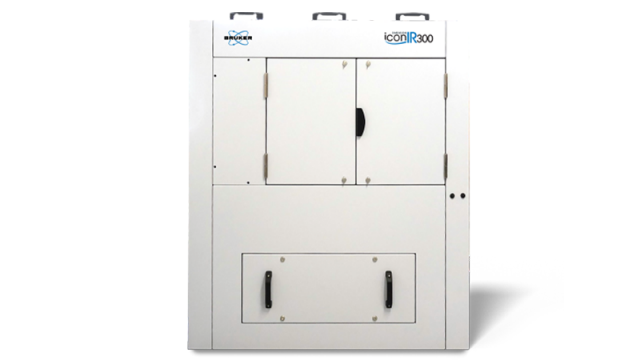
Image Credit: Bruker Nano Surfaces and Metrology
Whole-Wafer Measurement of 200 mm and 300 mm Wafers
Combining a unique, patented suite of AFM-IR modes and proprietary PeakForce Tapping® property mapping modes with its large sample architecture, the IconIR300 provides ultimate sample flexibility for the broadest semiconductor applications.
The system can perform whole-wafer measurements on samples up to 300 mm in diameter, accommodating a wide range of thicknesses and material types.
- Data storage media wafers
- Both organic and inorganic samples
- Bare wafers
- Patterned wafers and
- Photomasks
The IconIR300's Surface Sensitive AFM-IR mode provides unique and reliable chemical measurements of the surface of polymeric films deposited on semiconductor materials.
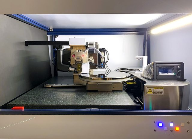
Interior view of the Dimension IconIR300 system during defect inspection of a 300 mm wafer. Image Credit: Bruker Nano Surfaces and Metrology
Highest Performance Nanoscale IR Spectroscopy for Semiconductor Applications
Bruker is a pioneer in photothermal AFM-IR-based nanoIR spectroscopy, a technique widely recognized as the preferred standard within the nanoIR community.
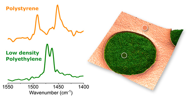
High-quality resonance-enhanced AFM-IR spectra collected at different sites on a PS-LDPE polymer blend, illustrating a high degree of material sensitivity and deeper insight into nanoscale material properties. Image Credit: Bruker Nano Surfaces and Metrology
Dimension IconIR300 Delivers
- Highly accurate, detailed spectra with FTIR correlation, enabling nanometer-level measurement of thin contaminants
- Advanced operational modes that support a wide range of sample measurements for both industrial and academic applications
- Industry-leading AFM-IR spectroscopy, delivering the highest performance in semiconductor nanoIR applications
- Reliable, surface-sensitive chemical analysis for polymeric films
Highest Resolution Chemical Imaging on Wafers and Photomasks
The Dimension IconIR300 combines industry-leading AFM performance with Bruker’s patented Tapping AFM-IR imaging to enhance the spatial resolution and sample accessibility of its nanoIR technology.
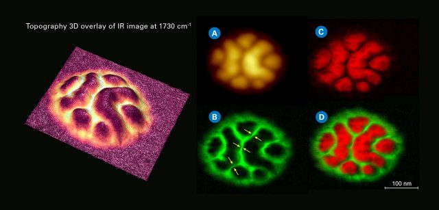
High-resolution chemical imaging of PS-b-PMMA block copolymer in Tapping AFM-IR mode showing sample topography (a); IR images at 1730 (b); and 1492 cm-1 (c) highlighting PMMA and PS, respectively. The yellow arrows in panel (b) indicate chemical resolution <10 nm. The overlay image (d) captures the composition map. Image Credit: Bruker Nano Surfaces and Metrology
Dimension IconIR300 Provides
- <10 nm chemical spatial resolution for imaging across a broad range of sample types, including soft organic and inorganic contaminants
- Consistent, reliable, and high-quality data
- AFM-IR technology that eliminates mechanical artifacts, ensuring accurate chemical composition measurements only
Advanced Automation for Identification of Nano-Contaminants
Equipped with the proprietary AutoMET® software suite, the IconIR300 provides multiple levels of automation for non-destructive AFM measurement. The system can be used on various sample types in real-time and offline.
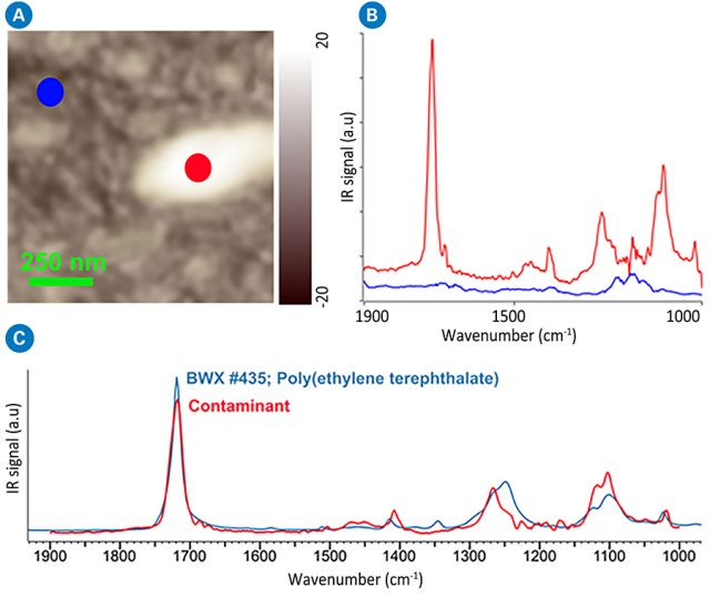
Height image (a) and resulting Photothermal AFM-IR spectra (b) from a contaminant on a bare silicon wafer. The resulting match from the FTIR library identifies the contaminant as Polyethylene terephthalate. Image Credit: Bruker Nano Surfaces and Metrology
Key Automation Capabilities Include
- Step-height analysis combined with nanoscale material property mapping
- Optical and AFM image pattern recognition
- Tip-centering
- Full-wafer and grid mapping support
- Image placement accuracy within tens of nanometers
- Intuitive recipe creation for simplified workflows
- KLARF file import capability to enable advanced nanoIR automation features
This technology combines nanoscale chemical characterization with highly resolved IR spectra to help academic and industrial users overcome the limitations of traditional defect identification on semiconductor materials.