Progress in quantum computing over the last 10 years has been staggering.
In 2018, quantum computing researchers and manufacturers struggled to produce devices with more than a few qubits. The best coherence times achieved for superconducting devices were barely above 100 microseconds.
Current superconducting quantum computers, like Fujitsu's 256-qubit system,1 now feature several hundred qubits and can achieve coherence times of over 1 millisecond. These advances show a tenfold increase in both qubit quality and scalability in less than a decade.
Similarly rapid progress has been observed across quantum, including photonic, cold atom, ion trap, spin, and color centers.

Image Credit: University of Nevada
As companies continue to pop up and areas like the Chicago Quantum Exchange compete to become the home of the future quantum industry, it’s worth considering the core challenges and promising solutions in scaling quantum systems.
For example, qubit counts today are still orders of magnitude below the tens of thousands required for most commercial applications, despite progress in the field.

Image Credit: University of Nevada
This progress has been hindered by the challenges in achieving the qubit quality required to make use of such massive systems, as well as the difficulties in interconnecting large numbers of qubits.
Differences exist across modalities, but quantum systems generally require two-qubit gates for entanglement: one-qubit gates for manipulation, one for read-out.
Each of these operations has an error rate, and the quantum computing community typically considers fidelity to be the inverse of the error rate.
Gates must be performed thousands of times on each qubit in most cases. The leading contemporary commercial systems offer fidelities in the range of 99.5 % for two-qubit gates2 and 99.99 % for one-qubit gates.3
In combination with emerging error-correction schemes, these rates enable systems to be operated with hundreds of qubits. This is impressive, but still far from the tens of thousands of qubits required for potential future applications.
These figures primarily refer to superconducting systems, but these challenges in performance and scale are present across modalities.
Image Credit: University of Nevada
None of this is a surprise, however. DARPA, a major scientific funding agency in the United States, recently announced a group of 16 (soon to be 18) companies selected for the Quantum Benchmarking Initiative, a three-stage program seeking to identify quantum computing architectures with the greatest potential to achieve utility-scale performance. This program includes a wide range of large and small companies across North America and Europe, including Rigetti Computing.4
Similar efforts are ongoing around the world, with governmental agencies and investors alike encouraging industrial and academic quantum researchers to focus on scale and performance, two factors that must evolve in tandem in order for the field to reach maturity.
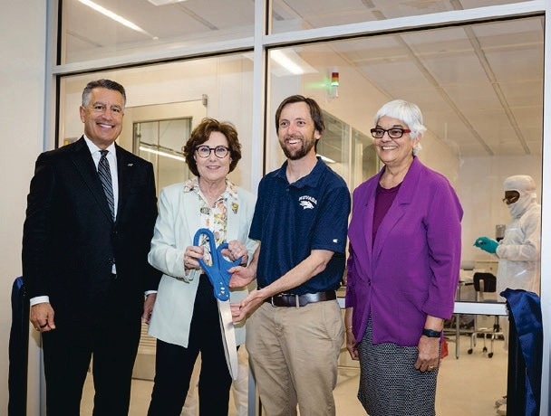
Image Credit: University of Nevada
Dr. Russ Renzas was at Rigetti Computing from 2016 to 2018, where he worked to develop a superconducting qubit fab and enhance device fabrication research efforts.
Most workers in the field at that time were from the physics community, but Dr. Renzas was a surface scientist.
As such, Renzas was focused on the first few nanometers of a dynamic environment, which frequently encountered issues of amorphization, oxidation, and contamination. Even crystalline surfaces can rearrange under the influence of chemistry and heat, with many materials behaving differently than in their bulk form.
When he left Rigetti, Dr. Renzas spent three years working at Oxford Instruments as a quantum technology specialist in the Plasma Technology sector, learning about other quantum modalities, liaising with Oxford customers worldwide, and looking into how Oxford products could address some of the field’s major challenges.
This unique role showed him that almost every type of quantum device faces the same two challenges: interfacial loss and 3D interconnection, as well as performance and scale.
Interfacial losses are a significant issue in quantum devices. Information in quantum devices is stored in the states of individual spins, photons, or electrons, meaning that any interaction with the spin, photon, or electron that affects its state can disturb or effectively erase quantum information.
Photonic quantum computers are more sensitive to photon loss than their classical counterparts. These computers regularly employ emerging nonlinear optoelectronic materials, such as lithium niobate, which can be difficult to etch.
Waveguide surface roughness can also cause losses in these systems. Superconducting quantum computers use meandering superconducting LC resonators, facing losses at every interface, including the metal-substrate, metal-air, and substrate-air interfaces.
A comparatively small degree of loss occurs from the interaction of the electromagnetic field with the bulk substrate and superconducting metal. Baths of unwanted states with unpredictable properties can be formed due to oxidation, roughness, contamination, interdiffusion, and amorphization at interfaces; however, this potentially perturbs the quantum information.
These unwanted states lead to unexpected behavior, for example, unpredictable coherence time fluctuations on the order of hours or even days.

Image Credit: University of Nevada
More attention has been paid to improving these interfaces in recent years. The community is turning to new base metals due to their lower losses. These metals, such as tantalum, offer reduced surface oxidation while benefiting from the more favorable properties of the non-superconducting oxides still present.
Several groups have also explored surface passivation as a means of reducing losses, using thin non-oxidizing surface layers of materials, such as gold. Systems continue to exhibit far more loss than is desirable or acceptable, however, despite these advances.
This is partly because, although these material systems reduce loss at the metal-air interface, electric fields interact much more strongly with corners and sidewalls than with top surfaces.
Corners and sidewalls can also be damaged by etch processes because traditional continuous etch processes dump significant amounts of physical and chemical energy into every surface they touch.
Superconducting or photonic waveguide top surfaces will be protected by a mask during etch, but sidewalls do not benefit from this protection.
Conventional plasma etch results in sidewalls and etch-exposed surfaces (for instance, the underlying substrate surface) that generally feature a damaged region extending 1-10 nm into the material, depending on the specific etch parameters employed.
For example, this damaged region is generally comprised of a mixture of Si-F, with surface roughness exceeding 1.0 nm RMS in the well-studied case of silicon in SF6 etches. The rough and disordered region may also be prone to increased oxidation versus unetched surfaces, depending on the etch chemistry and material.
However, this problem can be solved. Etch-induced damage directly scales with the physical and chemical energy dumped into the system throughout the etch process.
Atomic layer etch (ALE) is an alternative etching approach whereby a surface region is selectively modified in order to increase its volatility relative to the bulk.
The modified region is then selectively removed by supplying sufficient physical or chemical energy to remove the modified layer, without sufficient energy to remove or significantly perturb any unmodified material below.
ALE has been shown to improve device performance. A 2007 study saw researchers investigating InAs high electron mobility transistors, demonstrating enhanced Schottky gate diode characteristics and Hall mobility using ALE.5
Dr. Renzas delivered more than 100 talks on ALE’s potential to improve quantum device performance during his Oxford tenure, and most recently, two research groups presented compelling evidence of quantum device performance improvement using ALE during a recent APS March Meeting.6,7
Reno has recently begun to emerge as a tech hub, with a particular focus on battery manufacturing.
The University of Nevada, Reno (UNR) has highlighted ALE as its main priority, recently installing an Oxford Instruments Cobra ICP RIE ALE system at the core of the Davidson Foundation Cleanroom, Northern Nevada's first academic nanofabrication facility.
The Davidson Foundation Cleanroom was opened in April 2025 at a ceremony attended by Oxford Instruments Western Region Account Manager Demetri Chrysostomou and US Senator Jacky Rosen.
The cleanroom’s team is focused on leveraging its Cobra system to develop new ALE processes for quantum-relevant materials.
The team will explore ALE’s potential to enhance the performance of quantum devices by reducing surface roughness and sub-surface etch-induced damage, and will examine novel ALE approaches that can accommodate difficult materials.
Its work will focus on the use of anisotropic ALE, which involves modifying the material to be removed using, in this case, a fluorinated compound before removing the material using a very low ion-energy Ar ion sputter that has been tuned far below the threshold for bulk material sputter etching.
This approach to ALE is nominally anisotropic, but existing literature suggests that it is possible to tune the exact degree of anisotropy by tuning pressure and ion energy, potentially allowing anisotropic ALE to be used as a post-processing step to smooth sidewalls and remove subsurface damage.
The cleanroom team will also explore multi-step, cryogenic, and hydrogenation-based modification processes, as well as building on previous work with high-speed bias-pulsed ALE (BP-ALE) processes from the University of Illinois and Argonne National Laboratory with support from Oxford Instruments.9
New ion species will be explored as an alternative to Ar+ to extend ALE to softer materials.
Pending grant proposals will hopefully allow the team to purchase an Oxford Instruments PlasmaPro ASP high-rate atomic layer deposition (ALD) system. ALD is key to addressing the other notable limitation to current quantum devices: the issue of scale.
Many quantum devices require sophisticated three-dimensional integration schemes for signal delivery. Conventional electronics benefit from the use of complex copper vias and multi-layer architectures, but copper is not appropriate for most superconducting or photonic quantum devices because it is neither a superconductor nor a dielectric.
Superconducting vias necessitate the metallization of at least several tens of nanometers in thickness to achieve sufficient critical current. This is also important for ensuring good shielding performance, depending on the application.
These vias must extend through the full thickness of the substrate in most cases, requiring conformal high aspect ratio depositions of challenging superconducting nitride materials.
UNR hopes to take advantage of the PlasmaPro ASP’s high deposition rate in conjunction with ultra-smooth sidewalls from cryogenic deep silicon etch processes performed on its Cobra, enabling the development of reproducible, manufacturable superconducting vias.
The team also hopes to use the PlasmaPro ASP to explore chemically based isotropic ALE processes and the use of ALD for quantum applications, which had been historically impractical or unachievable due to conventional ALD systems’ low deposition rates.
Dr. Renzas has long believed that the PlasmaPro ASP will be the ideal system for these use cases, even envisioning this before the system was publicly announced.
The Future
The future of quantum technology continues to shine bright. Progress has been significant in the 10 years since Dr. Renzas entered the field, with a range of talented individuals continuing to enter the field. He considers this community to be filled with many of the most creative and brilliant minds in the world.
The challenges are real, and it will not be easy to reach ten thousand qubits, while reaching one hundred thousand qubits is almost unimaginable at this point.
The pace of progress in the field and the sheer number of opportunities yet to be realized leave room for optimism, however. For example, the team at UNR believes that atomic-scale processing gives considerable reason for optimism, with the field barely scratching the surface of what is possible with interfaces.
References and Further Reading
- https://www.fujitsu.com/global/ about/resources/news/press-releases/2025/0422-01.html
- https://www.rigetti.com/news/ rigetti-computing-launches-84-qubit-ankaa-3-system-achieves-99-5-median-two-qubit-gate-fidelity-milestone
- https://blog.google/technology/ research/google-willow-quantum-chip/
- https://www.darpa.mil/research/ programs/quantum-benchmarking-initiative
- Kim, T.-W. ., et al. (2007). Fabrication of InAs composite channel high electron mobility transistors by utilizing Ne-based atomic layer etching. Applied Physics Letters, (online) 91(10). DOI: 10.1063/1.2780113. https://pubs.aip.org/aip/apl/article-abstract/91/10/102110/119273/Fabrication-of-InAs-composite-channel-high?redirectedFrom=fulltext.
- https://summit.aps.org/events/ MAR-T18/4
- https://summit.aps.org/events/ MAR-A33/8
- Dallorto, S., et al. (2019). Balancing ion parameters and fluorocarbon chemical reactants for SiO2 pattern transfer control using fluorocarbon-based atomic layer etching. Journal of Vacuum Science & Technology B, Nanotechnology and Microelectronics: Materials, Processing, Measurement, and Phenomena, (online) 37(5). DOI: 10.1116/1.5120414. https://pubs.aip.org/avs/jvb/article/37/5/051805/590489/Balancing-ion-parameters-and-fluorocarbon-chemical.
Acknowledgments
Produced from materials originally authored by Dr. Russ Renzas from the Davidson Foundation Cleanroom Research Faculty at the University of Nevada.

This information has been sourced, reviewed, and adapted from materials provided by Oxford Instruments Plasma Technology.
For more information on this source, please visit Oxford Instruments Plasma Technology.