Plasma ALD of silicon nitride is increasingly recognized as a transformative development for both GaN and SiC technologies. Both material platforms benefit from the use of SiN ALD to deliver stable, high-performance interfaces able to support manufacturing scalability and long-term device reliability.
The power electronics landscape is experiencing a transformative revolution, primarily driven by the increasing popularity of wide bandgap (WBG) semiconductors, such as silicon carbide (SiC) and gallium nitride (GaN).
These materials are setting new standards in performance, offering breakthroughs in thermal management, efficiency, and power density that had been historically impossible to achieve with conventional silicon-based semiconductors.
WBG semiconductors are powering applications across industries, enabling faster switching speeds, higher voltage handling, and reduced energy losses in applications ranging from renewable energy systems to consumer electronics and electric vehicles (EVs).
While GaN and SiC technologies are extremely promising, they are accompanied by unique challenges that limit their full implementation. For example, issues related to interface traps, surface states, and dielectric integration can directly affect the performance and reliability of devices built on these platforms.
The plasma-enhanced atomic layer deposition (Plasma ALD or PEALD) of silicon nitride (SiN) has emerged as a key means of addressing these challenges, providing the material quality and precision required for next-generation devices.
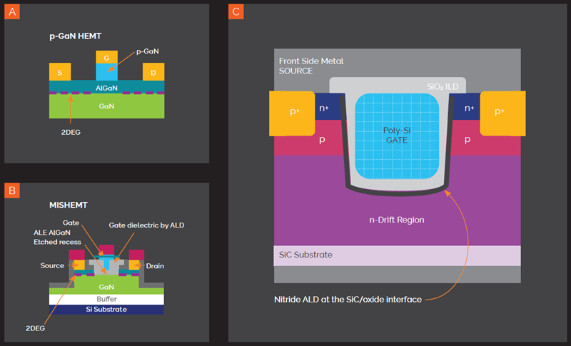
Key power device structures: A GaN High Electron Mobility Transistor (HEMT), B GaN Metal insulator HEMT (MISHEMT), and C SiC trench metal–oxide–semiconductor field-effect transistor (MOSFET). Image Credit: Oxford Instruments Plasma Technology
The Wide Bandgap Revolution
GaN Versus SiC
It is important to look at WBG semiconductors’ advantages over conventional silicon devices to better understand their transformative potential.
Silicon is ubiquitous in the semiconductor industry, but this material features underlying material constraints, including relatively low bandgap energy (1.1 eV), moderate breakdown strength, and limited thermal conductivity.
These limitations make it difficult to meet the demands of modern applications that require higher power density and higher efficiency.
The superior physical properties of wide bandgap materials, including GaN and SiC, allow them to overcome these limitations. For example, GaN features a bandgap of 3.4 eV, while that of SiC is 3.3 eV, allowing devices to operate at much higher voltages, frequencies, and temperatures. These properties translate into lighter, smaller, and more efficient power systems.
GaN and SiC share a number of benefits, but their use cases diverge considerably due to differences in their performance profiles and intrinsic properties.
GaN: The Low-Voltage Workhorse
GaN is widely regarded as the more suitable choice for low- to mid-voltage applications, generally under 1.5 kV. Its low gate capacitance and high electron mobility make it ideal for high-frequency switching, enabling efficient and compact designs.
GaN is a key material in applications such as consumer power supplies, fast chargers for mobile devices, RF amplifiers, and compact onboard chargers for EVs. Its ability to operate at high frequencies enables the development of smaller passive components, reducing power systems’ overall size and cost.
SiC: The High-Voltage Specialist
SiC is considered the material of choice for medium- to high-voltage applications, ranging from 3.3 kV to 33 kV.
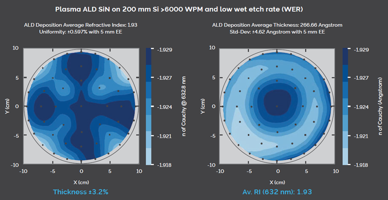
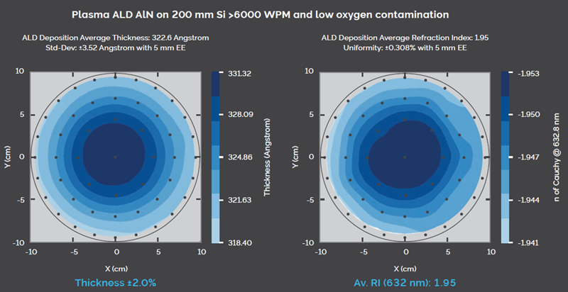
Silicon nitride ALD data from Oxford Instruments' Atomfab ALD system. Image Credit: Oxford Instruments Plasma Technology
Its exceptional robustness and thermal conductivity make SiC well-suited to use in harsh environments where reliability is essential. SiC-based devices also see routine use in renewable energy inverters, industrial motor drives, grid infrastructure, and EV traction systems.
High-voltage SiC MOSFETs and diodes are especially valued as they can accommodate extreme power levels with minimal energy loss. This characteristic makes them an essential tool in the integration of renewable energy sources into the grid and the electrification of transportation.
Shared Challenges: Surface States and Interface Engineering
GaN and SiC are unlocking new performance frontiers, but neither material is without its challenges. Both materials suffer from surface state and interface trap issues, the latter being localized energy states that form at the interface between the semiconductor and its dielectric layer.
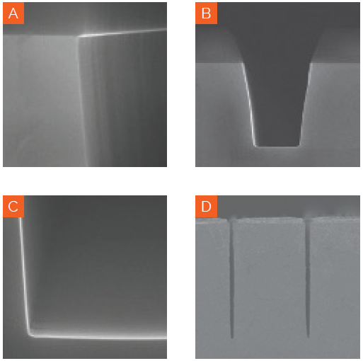
SiC superjunction trench (A, B, C) etch and high aspect ratio SiC superjunction trench etch (D). Image Credit: Oxford Instruments Plasma Technology
These traps have the potential to capture and release charge carriers, triggering undesirable effects such as threshold voltage instability, increased leakage currents, and reduced efficiency.
The quality of the interface between the GaN channel and the dielectric layer is critical for GaN devices, especially high-electron-mobility transistors (HEMTs). Uncontrolled surface states can result in dynamic on-resistance, reducing performance during high-frequency switching.
Similarly, the interface between SiC and thermally grown silicon dioxide (SiO2) is a well-known impediment in SiC MOSFETs, characterized by a high density of interface traps that cause threshold voltage drift and limit channel mobility.
Advanced materials and deposition techniques are needed to address these issues, allowing the creation of high-quality dielectric layers with minimal defects. Plasma ALD of silicon nitride (SiN) has emerged as a leading solution in this respect, facilitating the precise control of material properties and interface quality.
GaN Power Devices: Tackling Interface and Integration Challenges with Plasma ALD SiN
Achieving high performance in the evolving world of GaN power electronics depends on more than the choice of semiconductor.
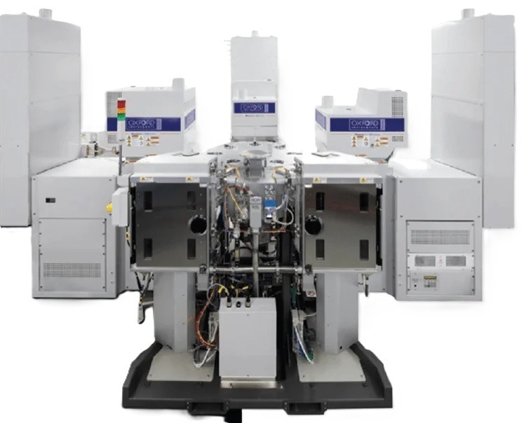
Oxford Instruments cluster system for compound semiconductor volume manufacturing. Image Credit: Oxford Instruments Plasma Technology
For example, supporting thin films, especially SiN, are key to enabling reliable operation and enhancing device behavior. SiN must perform multiple tasks simultaneously when functioning as a dielectric gate insulator, a passivation layer, or a moisture barrier, all while maintaining stability under both environmental and electrical stress.
Interface quality directly affects the key performance metrics of HEMTs. For example, it is essential to ensure the presence of a uniform, defect-free SiN layer on the GaN surface to suppress unwanted surface states that would otherwise destabilize threshold voltages, introduce charge traps, and degrade performance over time.
This is especially important in increasingly popular MISHEMT (metal-insulator–semiconductor HEMT) architectures to achieve normally-off operation. The dielectric-semiconductor interface becomes the focal point of long-term reliability and control in these devices.
There have been several recent studies into this area, including those led by prominent research institutes such as IMEC.1 This work has highlighted the value of high-quality nitride films in considerably reducing the density of interface traps (Dit) on GaN.
A reduction in trap density leads to reduced hysteresis, more stable electrical characteristics, and improved operational robustness. These are key advantages for devices intended for use in high-reliability applications, including aerospace and automotive settings.
Conventional SiN deposition techniques have posed major challenges to wide-scale implementation, however. While operating at relatively low temperatures, early ALD processes have limited suitability for high-volume production due to their slow growth rates and lengthy cycle times.
Legacy techniques such as low-pressure CVD (LPCVD) have produced dense and highly etch-resistant films, but these techniques have required processing temperatures that typically exceed 700 °C. These temperatures limit downstream integration flexibility due to being incompatible with GaN device stacks.
Oxford Instruments has developed a PEALD process for SiN in order to address this technological gap, successfully combining high deposition rates, high film quality, and low processing temperatures.
This approach facilitates the growth of high-quality SiN films at temperatures below 300 °C, meaning it is fully compatible with modern integration flows and advanced GaN architectures.
A notable characteristic of this process is a low-damage plasma pre-treatment capable of gently preparing the GaN surface by removing native contaminants and oxides without damaging the underlying crystal.
The subsequent SiN film demonstrates excellent conformality, even on high aspect ratio or otherwise complex structures, exhibiting a low wet etch rate that is comparable to conventional LPCVD films. This robustness ensures film integrity during downstream processing and packaging stages.
The platform is also engineered for manufacturing scalability, with the PEALD SiN process able to support wafers up to eight inches (200 mm) in diameter. This capability aligns with the industry's shift towards larger substrate sizes in the fabrication of power semiconductors.
Notably, it bridges the longstanding gap between quality and throughput, offering this capability while maintaining a cost-of-ownership (CoO) that is competitive with traditional CVD-based approaches.
GaN technologies continue to enter mainstream power markets, from increasingly compact automotive systems to high-efficiency chargers and fast converters. The potential to integrate high-quality SiN films with precision, speed, and reliability is a critical differentiator as this market penetration continues.
Plasma ALD has become more than a novel deposition technique; rather, it is now a fundamental enabler of the next generation of GaN-based power devices.
SiC Power Devices: Interface Engineering for Lifetime and Stability
SiC is becoming increasingly recognized as a key material in high-voltage power electronics, especially in applications exceeding 3.3 kV.
One of the most notable and longstanding challenges in SiC device engineering stems from the interface between the SiC substrate and the thermally grown (SiO2) gate dielectric. This junction has been recognized as a key limiting factor in device performance due to a high density of electrically active traps being present.2
These traps are detrimental to channel mobility and contribute to threshold voltage instability, switching increased gate charge, and hysteresis. This causes lower energy efficiency and greater conduction losses.
These effects undermine the consistency and long-term reliability of SiC-based power devices over extended periods of operation, particularly under high-stress conditions.
The industry has turned to advanced interface engineering solutions to help mitigate these limitations, with one of the most promising approaches being the introduction of a thin SiN interlayer between the SiC substrate and the SiO2 layer.
This SiN film functions as a dielectric buffer, improving the electrical characteristics of the interface. The film effectively suppresses the formation of interface traps, reducing the overall trap density by passivating dangling bonds on the SiC surface. This improvement leads to improved dielectric properties and greater threshold voltage stability, even at elevated temperatures and under prolonged bias.
The interlayer strengthens the electrical insulation while also reducing leakage current, ensuring predictable and robust performance. These enhancements are particularly valuable in mission-critical systems where long-term reliability and operational stability are paramount, such as railway traction modules, electric vehicle inverters, and power conversion units for the electrical grid.
PEALD enables the integration of this SiN layer into practical device architectures, providing atomic-level thickness control, which in turn ensures the precise deposition of ultra-thin dielectric layers and enables uniform, conformal film growth.
PEALD also offers lower energy exposure than other, more aggressive plasma processes, preserving the integrity of the SiC interface and reducing the risk of plasma-induced damage.
The method is highly compatible with modern gate stack designs, including nitride and oxide combinations. This compatibility allows the creation of custom dielectric stacks that can be optimized for key performance parameters, for example, breakdown voltage, switching speed, and thermal stability.
Device manufacturers adopting PEALD as a tool for interface engineering can fine-tune dielectric stacks for improved electrostatic control and reduced switching losses. This ability ultimately leads to enhanced endurance and improved efficiency in next-generation SiC power devices.
The deposition of SiN using PEALD is unlocking new opportunities in the SiC-based electronics field. Achieving near-perfect control at the dielectric interface will be essential as voltage demands and application complexity continue to rise.
Plasma ALD provides the scalability, material performance, and precision required to meet these evolving challenges in power electronics.
Summary
Wide bandgap semiconductors, such as SiC and GaN, are redefining the boundaries of power electronics, offering higher voltage handling, unrivaled efficiency, and thermal robustness.
GaN excels in low-to mid-voltage applications, including RF systems and fast chargers, while SiC is ideally suited to high-voltage applications such as electric vehicle traction systems and energy infrastructure.
Both materials face significant challenges, however, most notably related to interface traps, surface states, and dielectric integration. These limitations have the potential to hinder performance and reliability.
SiN deposited via PEALD has become recognized as an enabling technology able to address these issues. It serves as a versatile thin film in GaN devices, enabling moisture protection, passivation, and gate dielectric layers, while enhancing threshold voltage stability, improving reliability, and suppressing leakage.
A thin SiN interlayer acts as a buffer between SiC and SiO2 in SiC devices, stabilizing threshold voltage, reducing interface trap density, and ensuring reliable long-term operation under even extreme conditions.
Plasma ALD SiN is helping to solve these integration challenges, unlocking the full potential of GaN and SiC technologies and paving the way for the next generation of reliable, efficient, and scalable power devices across industries.
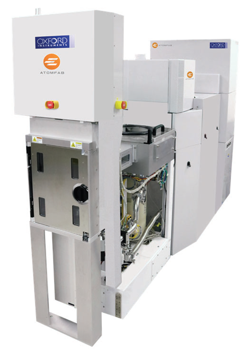
Oxford Instruments Atomfab system for high-rate volume manufacturing oxide and nitride ALD. Image Credit: Oxford Instruments Plasma Technology
Innovations like Plasma ALD are ensuring that WBG semiconductors continue to be at the forefront of technological advancement, as demand for high-performance power electronics continues to increase.
References and Further Reading
- Marcon, D., et al. (2015). Direct comparison of GaN-based e-mode architectures (recessed MISHEMT and p-GaN HEMTs) processed on 200 mm GaN-on-Si with Au-free technology. SPIE Proceedings, 9363, p.936311. DOI: 10.1117/12.2077806. https://www.spiedigitallibrary.org/conference-proceedings-of-spie/9363/936311/Direct-comparison-of-GaN-based-e-mode-architectures-recessed-MISHEMT/10.1117/12.2077806.short.
- Romano, G., et al. (2023). Investigation on Switching Characteristics of 3.3 kV SiC Power MOSFETs with SiO2/ SiN Gate Stack. Materials Science Forum, (online) 1091, pp.49–53. DOI: 10.4028/p-upzg90. https://www.scientific.net/MSF.1091.49?utm_source=researchgate.net&utm_medium=article.
Acknowledgments
Produced from materials originally authored by Dr. Aileen O'Mahony, Bas Derksema, and Grant Baldwin from Oxford Instruments Plasma Technology.

This information has been sourced, reviewed and adapted from materials provided by Oxford Instruments Plasma Technology.
For more information on this source, please visit Oxford Instruments Plasma Technology.