While GaN HEMT devices are fabricated in a wide range of designs, they all work by protecting and optimizing the critical 2DEG layer at the interface. This article looks at this particular device challenge, detailing plasma solutions that are applicable to the design of many GaN HEMT devices.
Today’s energy- and data-driven world has seen accelerated adoption of gallium nitride (GaN) devices in line with a reduction in costs throughout the power electronics industry.
GaN benefits from improved electron conduction efficiency and the capacity to withstand high electric fields compared to conventional silicon-based power devices. Such advantages have been successfully integrated in high-volume consumer electronics applications, including the manufacturing of smaller and faster mobile device chargers.
The GaN power device market revenue is anticipated to reach two billion dollars by 2027.1 This growth has been primarily driven by consumer applications, but the more widespread implementation of GaN power devices is expected in a wide range of markets, including renewable energy, electric vehicles, data centers, and infrastructure for 5G and 6G networks.
Despite GaN’s superior material qualities, the presence of the 2DEG (two-dimensional electron gas) results in GaN HEMTs being normally-on, known as depletion-mode (D-mode): this is extremely undesirable for power electronics applications. It is imperative that these devices are normally-off to ensure fail-safe operation, with a positive threshold voltage (Vth) achieved.
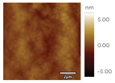
Figure 1. 50 % reduction in measured AlGaN roughness (0.4 nm Ra) with combined ICP & ALE process compared to ICP-only process (0.8 nm Ra). Image Credit: Oxford Instruments Plasma Technology
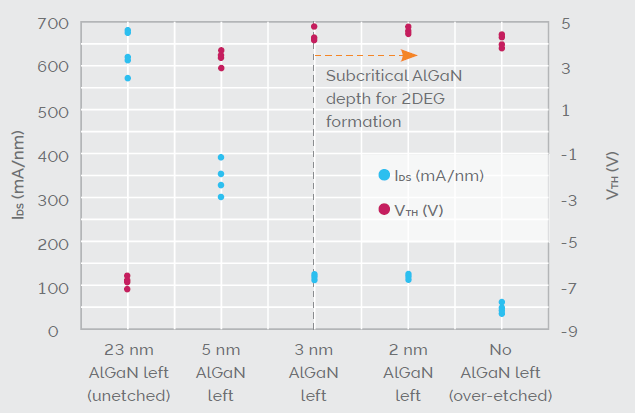
Figure 2. Correlation of Vth and on-state device current depending on the AlGaN remaining (measured by five devices of different locations). Image Credit: Oxford Instruments Plasma Technology
Multiple device architectures have been proposed to facilitate normally-off operation. Cascode (normally-on GaN HEMT integrated with normally-off Si MOSFET) and p-GaN HEMTs have been the most widely used of these approaches.
There are limitations associated with both device types, however. For example, cascode devices have been observed to add undesirable interconnect parasitic inductances, while p-GaN devices sometimes suffer from high gate leakage current.2,3
It is possible to improve p-GaN HEMT performance by ensuring precise control of p-GaN etch depth along with minimum roughness or damage to the AlGaN surface. This enables the development of higher performance normally-off HEMT devices with lower off-leakage, higher drive current, and improved dynamic on-resistance.4
Oxford Instruments has developed a combined etching and endpoint solution for p-GaN HEMTs. This solution leverages a combination of traditional inductively coupled plasma (ICP) etch and atomic layer etch (ALE) in order to offer improved etch control, reduced AlGaN roughness, and minimal loss of the AlGaN barrier (Figure 1).
An ICP etch process is used to remove the p-GaN layer with the high selectivity that is necessary to ensure minimal AlGaN layer loss. An ALE process is then introduced to reduce the AlGaN surface’s roughness.
The effectiveness of this solution is dependent on ensuring the interface to AlGaN is detected at precisely the optimal point to allow switching to the high selectivity ICP process to minimize the AlGaN loss.
This is made possible via the patent-pending Etchpoint™ endpoint detector, an exclusive LayTec product developed in partnership with Oxford Instruments.
A gate recessed metal-insulator-semiconductor high-electron-mobility transistor (MIS-HEMT) is another important and beneficial device type. This device can achieve positive threshold voltages (Vth) and high gate voltage swing, while reaching higher breakdown voltages and enabling the use of simple gate driving circuitry.2
A major challenge for gate recessed MIS-HEMT is ensuring the precise monitoring and control of the etch to leave a ≤ 5 nm layer of AlGaN. This generally requires sub-nanometer level control in the remaining AlGaN layer to ensure repeatable positive Vth while maintaining a 2DEG.
It is possible to form a recessed MIS-HEMT by thinning the AlGaN barrier in the gate region to achieve a normally-off device with a gate dielectric (for example, Al2O3 by atomic layer deposition) deposited to reduce leakage current.
The realization of reproducible and stable recessed MIS-HEMTs necessitates the use of a precise, controllable, and repeatable low-damaging etch process able to ensure a high-quality dielectric with minimal defects and minimal interfacial traps.
ALE is the ideal solution when etching < 30 nm of an AlGaN layer to a critical depth specification to form a partially recessed gate MIS-HEMT, because this technique delivers a controlled low etch rate, low damage, and high uniformity versus conventional ICP etching.
The final necessary capability is the ability to halt the etching process at exactly the right AIGaN etch depth and time within the AlGaN etch process, accounting for an incoming AlGaN layer with varying thickness.
Optical end pointing is especially challenging because the film thicknesses involved are generally small fractions of the wavelength of light.
Alternative endpoint technologies are available, but these technologies have only limited accuracy (> two nm) in terms of their capacity to repeatably determine the amount of AlGaN remaining on the GaN layer.
Using Etchpoint, Oxford Instruments has developed the ability to monitor the etch depth and stop the process with ± 0.5 nm of the remaining AlGaN thickness specification, ensuring that the target Vth can be achieved for normally-off behavior.
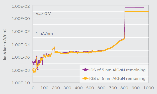
Figure 3. Off-state breakdown voltages of 5 nm AlGaN remaining (LGD = 10 μm). Image Credit: Oxford Instruments Plasma Technology
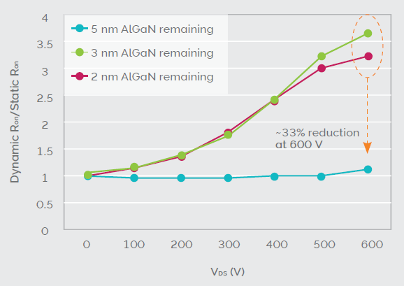
Figure 4. Dynamic Ron/ Static Ron ratio by the AlGaN remaining thickness variation VGSQ = -5 V, VDSQ = 0 V, 100 V, 200 V, 300 V, 400 V, 500 V, 600 V at 0.1ms (pulse width: 500 μs). Image Credit: Oxford Instruments Plasma Technology
When used in conjunction with Etchpoint in situ monitoring, Oxford Instruments’ highly controlled, low-damage ALE process delivers excellent etch control of the thin AlGaN barrier layer in the gate recess area.
A recent study involved etching a range of AlGaN thicknesses, from five nm AlGaN remaining, through to an over-etch into the AlGaN barrier. This facilitated the investigation of the impact of etching on the resulting device performance, with the aim of achieving normally-off MIS-HEMTs.
Transmission electron microscopy (TEM) was used to confirm that the accuracy and repeatability of achieving the target five nm remaining thickness of AlGaN was less than ± 0.5 nm.5,6 TEM post-etch measurements were found to correlate strongly with real-time in situ Etchpoint thickness measurements.
Figure 2 features four different thicknesses of AlGaN barrier and the related effect on the Vth and on-state drain current. Published data shows that 2DEG effects are hardly observed under three nm of the remaining AlGaN layer, meaning that an accurate AlGaN target thickness and endpoint solution are key to achieving 2DEG formation. 7
Devices with five nm of AlGaN remaining were shown to exhibit +3.4 Vth, 2.22 mΩcm2 of specific on-resistance (Ron), and 830 V of off-state breakdown voltage at one μA/mm (Figure 3). Devices with five nm of AlGaN remaining were also shown to demonstrate a 68 % reduction at 600 V of the dynamic Ron/static Ron ratio versus cases with two nm and three nm of AlGaN remaining.
The higher ratio of dynamic versus static on-resistance shown in devices with an AlGaN layer of ≤ three nm AlGaN features a higher trap density due to the anticipated degradation of the thin AlGaN surface that is likely due to the formation of an oxide layer (Figure 4).8
When used in conjunction with Etchpoint, Oxford Instruments’ ICP and ALE solutions deliver excellent etch control and low damage processing, delivering notable device performance benefits for both p-GaN HEMTs and gate-recessed MIS-HEMTs.
These capabilities are integrated on the industry-proven PlasmaPro® 100 Cobra platform, allowing the company’s customers to repeatably and reliably manufacture GaN devices for emerging applications with a keen focus on reduced global environmental impact via lower power consumption and improved efficiency.
References and Further Reading
- Yole Intelligence “2021 Status of Power Electronics Market” and “Power GaN 2022.”
- Zhang, C., et al. (2022). Hybrid Gate p-GaN Power HEMTs Technology for Enhanced Vth Stability. 2022 International Electron Devices Meeting (IEDM), (online) pp.35.4.1–35.4.4. DOI: 10.1109/iedm45625.2022.10019437. https://ieeexplore.ieee.org/abstract/document/10019437.
- Xia, F., et al. (2021). Investigation of high threshold voltage E-mode AlGaN/GaN MIS-HEMT with triple barrier layer. Results in Physics, 25, pp.104189–104189. DOI: 10.1016/j.rinp.2021.104189. https://www.sciencedirect.com/science/article/pii/S2211379721003363?via%3Dihub.
- Zhang, P., et al. (2022). High Selectivity, Low Damage ICP Etching of p-GaN over AlGaN for Normally-off p-GaN HEMTs Application. Micromachines, 13(4), p.589. DOI: 10.3390/mi13040589. https://www.mdpi.com/2072-666X/13/4/589.
- S.J. Cho et al, presented at 14th International Conference on Nitride Semiconductors 2023.
- Oxford Instruments. (2026). Enabling reliable normally-off recessed gate MISHEMT fabrication for power electronics applications White Paper - Oxford Instruments. (online) Oxford Instruments. Available at: https://plasma.oxinst.com/media-centre/wp/ale-and-etchpoint-for-gan-recessed-gate-mishemt.
- Brown, R., et al. (2014). A Sub-Critical Barrier Thickness Normally-Off AlGaN/GaN MOS-HEMT. IEEE Electron Device Letters, 35(9), pp.906–908. DOI: 10.1109/led.2014.2334394. https://ieeexplore.ieee.org/document/6856144.
- M. S. Miao et al. (2010). Oxidation and the origin of the two-dimensional electron gas in AlGaN/GaN heterostructures. Journal of Applied Physics, 107 123713. DOI: 10.1063/1.3431391. https://pubs.aip.org/aip/jap/article-abstract/107/12/123713/146167/Oxidation-and-the-origin-of-the-two-dimensional?redirectedFrom=fulltext.
Acknowledgments
Produced from materials originally authored by Dr Aileen O'Mahony from Oxford Instruments, Dr Sun-Jin Cho, Dr Tania Hemakumara, and Dr Matthew Loveday.

This information has been sourced, reviewed and adapted from materials provided by Oxford Instruments Plasma Technology.
For more information on this source, please visit Oxford Instruments Plasma Technology.