The drive to cut the cost of making silicon carbide (SiC) power devices continues to shape the industry. Much of the focus has fallen on substrate supply and cost, the shift to trench device designs, and the rollout of automated 200 mm foundries.
One of the best-known and most costly challenges in making silicon carbide (SiC) MOSFETs is creating a high-quality, reliable oxide layer on the SiC surface. Where that cannot be fully achieved, manufacturers must rely on processing techniques, device design, and testing to reduce the impact of an imperfect oxide.
Like silicon, SiC can be oxidized to form silicon dioxide (SiO2). This is considered one of the most notable advantages of SiC as a wide bandgap semiconductor, but SiC’s carbon content is known to convolute the simple oxidation process.
Carbon can become trapped, both within the oxide and at the interface between the oxide and SiC. It is important that this imperfect oxide be managed with a nitric oxide anneal to deliver a high enough quality oxide suitable for the mass market.
This gate oxide has underpinned several SiC innovations. For example, trench device architectures overcome a high channel resistance triggered by the gate oxide.
As many as a quarter of gate oxides fail immediately following fabrication. This presents a significant issue in terms of device yield and cost, necessitating the implementation of a burn-in testing stage to identify the rogue devices.
Device designers must also protect a SiC MOSFET's gate oxide at all costs to ensure longer-term reliability. This consideration dictates device design choices and typically necessitates derating.
This article looks at the origin of this problem, looking at how carbon that is not fully removed in the oxidation of SiC can impact yield, efficiency, and reliability. State-of-the-art nitrogen-based processing techniques that support the delivery of transformative SiC product ranges will also be evaluated.
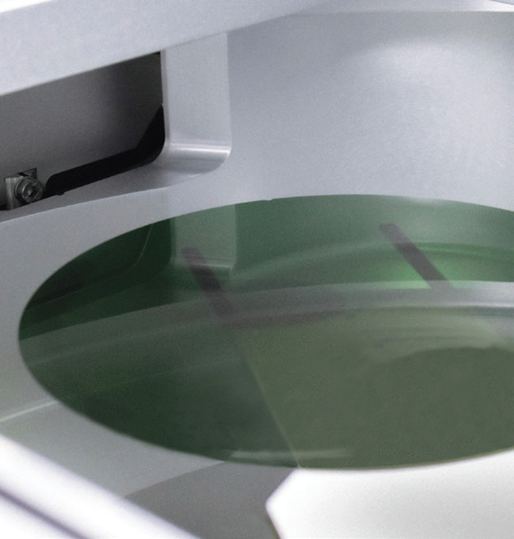
200 mm SiC substrates burst onto the power semiconductor technology landscape in 2023. Image Credit: Oxford Instruments Plasma Technology
Silicon Carbide and Its Similarity to Silicon
Driven by demand from the industrial machine, electric vehicle, data center, and renewable energy sectors, the silicon carbide (SiC) device market is currently worth $3 billion per year, a dramatic rise since the release of the first SiC MOSFET in 2011.
This growing demand is driven by the material’s core properties, including high thermal conductivity, a high critical electric field and a wide bandgap. Together, these characteristics enable the fast switching and high-efficiency power converters for which SiC is now well known.
Most of these properties are shared by other wide bandgap semiconductors, however, including diamond, gallium nitride, and gallium oxide.
SiC stands apart from these other wide bandgap materials due to its similarity to silicon (Si) in two notable ways.
Like Si, it is possible to grow high-quality, large-area boules (cylinders) of SiC that can be cut into individual freestanding substrates. The fabrication process can then begin on these substrates, which remain very expensive due to slow growth times, limited achievable SiC boule heights, and large equipment and maintenance costs.
The multi-billion dollar industry-wide transition from a technology based on 150 mm diameter substrates to one based on 200 mm ones is expected to be a key driver in projected cost reduction.
The second parallel between SiC and Si is their potential to form a layer of silicon dioxide (SiO2) on each of their surfaces via the thermal oxidation process. SiC is 50 % silicon, meaning that heating its surface in oxygen to temperatures between 1200-1400 °C results in the formation of SiO2, which is the ideal insulator for the formation of a functional, reliable MOSFET.
These parallels mean that SiC power devices (MOSFETs, Schottky diodes, JFETs) are close to exact copies of the Si devices developed over 50 years ago. Indeed, for example, it would be difficult to identify any clear differences between a 200 V Si MOSFET and a 1200 V SiC MOSFET.
SiC and its oxide are complex, however. Being a compound with 50 % silicon content offers a range of benefits, but the role its carbon plays in the oxidation process is the underlying cause of its widely recognized limitations in terms of reliability, device yield, and efficiency.
Hundreds of PhD theses over more than three decades have explored the challenge of optimizing the interface between SiC and SiO2 to minimize losses and improve reliability.
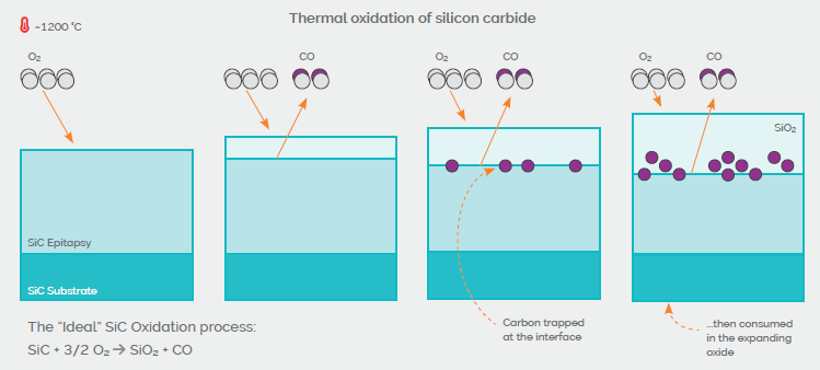
Figure 1. The thermal oxidation of silicon carbide results in a SiO2 layer forming on its surface. As this progresses, however, carbon gets trapped at the SiC/SiO2 interface and within the SiO2 itself. Image Credit: © PGC Consultancy Ltd 2024
The SiC Oxidation Process
Figure 1 illustrates the SiC thermal oxidation process occurring in a tube furnace as oxygen is passed over substrates of SiC at temperatures between 1100 and 1400 °C.
This process begins with a simple chemical reaction, which sees oxygen binding with Si from the SiC surface to form the initial SiO2 monolayers. The carbon also reacts with oxygen, forming carbon monoxide (CO), which will be removed as a byproduct.
After this initial layer has grown, incoming oxygen permeates the thin SiO2 layer already formed, with further Si from the SiC also consumed to form a deeper,
thicker layer of SiO2. Most of the carbon travels through the thin SiO2 layer and is removed. Within just a few monolayers of SiO2 growth, however, there is evidence of trace carbon amounts that do not depart through the SiO2.
Figure 1 shows that unreacted carbon atoms are trapped at the interface between the SiC and the newly formed SiO2.
This interfacial carbon causes significant issues, but the interface is still in motion at this stage as more SiC is consumed during the ongoing oxidation process. Carbon that may have been released at the interface is itself consumed within the expanding oxide, where it remains.
Once the thermal oxidation process has been completed and a layer of around 40 nm of SiO2 has been formed on the SiC surface, the resulting layer is not the pure SiO2 required for silicon device processing. Rather, this now-permanent SiO2/SiC interface features unwanted carbon throughout the oxide.
The Trapped Carbon Problem
The MOS interface featuring the newly formed SiO2 gate oxide is key to MOSFET transistor operation, but the presence of trapped carbon has a significant adverse effect in three key areas related to reliability, efficiency, and yield.
Figure 2 shows the ‘channel,’ a region formed within the top few nanometers of the SiC upon the application of a gate voltage. This region has a central role in the operation of a MOSFET, allowing a flow of charge (electrons) through the device when it is on, blocking this current when the device is off, and efficiently and reliably transitioning between these two states.
Electrons pass through this narrow channel during the ‘on’ state, remaining in intimate contact with the oxide interface. This makes its quality of vital importance.
This semiconductor-based channel can be understood as similar to water passing through a canal, and the impact of the carbon residing at the interface can be likened to several thousand boulders or other objects blocking the canal and slowing down the stream of water.
The flow of electrons beneath the gate oxide is also impeded by the trapped carbon, but this is more than a physical barrier from the interfacial carbon.
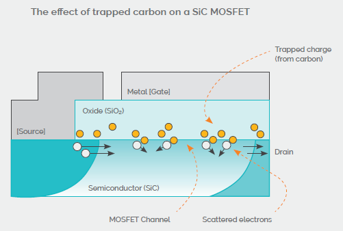
Figure 2. Carbon related charge located at the SiC/SiO2 interface and within the oxide cause electrons to be slowed and diverted from their ideal path, a process that leads to low channel mobility, high channel resistance, and conduction losses (inefficiency). Image Credit: © PGC Consultancy Ltd 2024
Each atom of unwanted, trapped carbon, whether this is at or close to the interface, will possess an amount of electrical charge that will exert a force on the stream of electrons passing beneath it (Figure 2).
These phenomena are referred to as interface and near-interface traps. The greater the density of unwanted carbon present throughout the oxide, the slower the electron flow and the higher the MOSFET's resistance. The flow of electrons in a semiconductor is measured via ‘electron mobility.’
The electron mobility in the channel of a silicon MOSFET is generally higher than 400 cm2/V.s. In SiC, however, the trapped charge means that its electron mobility may be as low as 5 cm2/V.s.
This 80x reduction in mobility reduces device efficiency, leading to an 80x increase in channel resistance. Channel mobilities this low would not be able to deliver today’s efficient SiC devices.
Today’s State of the Art: Nitrogen
SiC gate-oxide issues have been recognized since the demonstration of the first SiC MOSFETs in the early 1990s. PhD students and research scientists have since investigated a wide range of potential solutions designed to reduce carbon trapping, lower device resistance, and increase channel mobility.
Research into boosting channel mobility has historically focused on different deposition methods, SiC polytypes, crystal planes, dielectric materials, substrate off-cut angles, and the role of material defects.
Many studies have considered the impact of introducing other elements into the oxidation process, including phosphorus, boron, sodium, arsenic, antimony, and caesium. Some of these studies yielded high channel mobilities of >100 cm2/V.s, but there were also unintended consequences in terms of yield or reliability.
The most successful solution found in this body of work is the utilization of nitrogen in the oxidation process.
This process involves the direct oxidation of SiC in nitric oxide (NO) as opposed to oxygen, or performing a conventional oxidation in O2 before carrying out a post-oxidation anneal in NO.
Direct oxidation in NO yields the highest mobility, but this method is slower, prompting manufacturers to generally favor the post oxidation anneal approach. The nitrogen bonds to unattached silicon at the interface in both cases, reducing the charge at the interface and generally boosting mobility to 25-35 cm2/V.s.
The NO post-oxidation anneal is widely utilized by device manufacturers because its resulting mobility value is just high enough to be viable. Modeling carried out by Oxford Instruments in a state-of-the-art 750 V SiC MOSFET has shown that the channel accounts for between 10 and 20 % of the total device resistance, depending on the specific design in question.
SiC channel mobility is still an order of magnitude lower than the equivalent silicon value; however, Oxford Instruments’ modeling suggests that an improvement to around 100 cm2/V.s will virtually eliminate this resistance.
Improvements in channel mobility are key drivers for efficiency gains and resistance reductions that eventually lead to die shrink and yield improvement. This is just one aspect of the gate oxide issue, however, which also impacts long-term reliability and production yield.
Oxide-Related MOSFET Reliability
Utilizing nitrogen-based post-deposition anneals within the oxidation process is effective, and this approach has been successfully transferred to the industrial environment. It is unable to entirely heal the imperfect oxide formed on SiC, however.
Because carbon remains throughout the entire oxide, rather than solely at the interface, this results in fixed and mobile charge states in the oxide itself. These charge states affect MOSFET function, leading to a range of reliability challenges.
For example, if the oxide is exposed to too much stress over too long a period, this can result in long-term vulnerability to failure. There is, therefore, a need to produce designs able to ‘protect’ the gate oxide from high electric fields within the device, as well as the derating of the device, whereby conservative device design is used to ultimately reduce efficiency in order to limit stress.
This oxide also exhibits several other characteristics, including its threshold voltage (the gate voltage required to turn on the device), which potentially drifts up or down as a result of applying a voltage to the gate.
Connecting multiple devices in parallel to increase current throughput (for example, in automotive applications) requires careful management to avoid mismatched threshold voltages. These unmatched voltages can lead to uneven wear and ultimately result in premature device failure.
There has been rapid progress in these areas in recent years, and these issues are now considered to be under control.
Derating and other mitigation strategies have been successful, meaning that threshold voltage instability is no longer a major issue when devices are employed within the safe conditions specified on an automotive-qualified MOSFET datasheet. The limitations imposed to achieve this are restrictive, however.
Oxide-Related MOSFET Yield Issues
Gate oxide failures are the most significant source of yield loss in the device fabrication process, overshadowing failures from substrate defects, and represent one of the biggest challenges for chip manufacturers.
Some manufacturers immediately write off as many as 25 % of fabricated MOSFETs post-fabrication due to extrinsic device failures originating from the gate oxide. This is referred to as ‘infant mortality’ and is essentially a reliability issue that is caught early, with devices failing due to imperfections in this essential layer.
This means that every finished device must be tested post-fabrication in order to identify all devices that will fail immediately.
Silicon processing gives so few failures that this process is unthought of, but the SiC industry is increasingly turning to burn-in testing, loading 18 fully processed SiC wafers into a chamber, and testing each device on the finished wafer in parallel, stressing the device (applying a voltage to the gate) for 48-96 hours to prompt those with issues to immediately fail.
IDMs can use this knowledge to eliminate bad die on the wafer prior to dicing and subsequent module development or packaging.
There is an ongoing debate around the cause of extrinsic gate oxide failures. The high electric fields in SiC and the lower potential barrier between SiC and SiO2 are believed to be one possible cause, but the presence of defects in the oxide represents an ever-present touchpoint for theories and models seeking to explain gate oxide failures.
Summary
Contemporary nitrogen-based oxide processing has seen SiC device fabrication develop from the poor interface with low mobility initially identified in the early 1990s. The industry has developed ways to address the connected yield and reliability issues, rendering these devices sufficiently efficient.
This has sufficient capacity to underpin an automotive-qualified product portfolio that is revolutionizing electric vehicle power supplies, but there is still scope to strive for a solution able to enhance yield, long-term reliability, and efficiency by tackling the root cause of these issues: the carbon problem.
References and Further Reading
- Yole, Capacity expansion and 200mm transition are driving a $30B investment rush today for a $10B SiC market by 2029 https://www.yolegroup.com/ product/report/power-sic---markets-and-applications-2024/
Acknowledgments
Produced from materials originally authored by Prof. Peter Gammon from Warwick University and PGC Consultancy.

This information has been sourced, reviewed, and adapted from materials provided by Oxford Instruments Plasma Technology.
For more information on this source, please visit Oxford Instruments Plasma Technology.