A defining focus of Oxford Instruments’ work is driving progress in compound semiconductor technology.
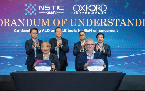
Official opening ceremony of the National Semiconductor Translation and Innovation Centre for gallium nitride. Image Credit: Oxford Instruments Plasma Technology
The company boasts one of the world’s leading facilities for the development of these revolutionary devices. It’s unlocking higher energy efficiency, improved thermal performance, higher power, and greater optoelectronic properties that are simply not possible with traditional silicon semiconductors.
Its customers range from start-ups to high-volume manufacturers, all using Oxford Instruments’ technology to advance augmented reality, power devices, three-dimensional sensing, and the optoelectronic transceivers that support hyperscale data centers.
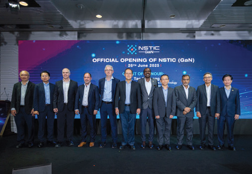
Image Credit: Oxford Instruments Plasma Technology
A notable example of Oxford Instruments’ global impact is the role that the company is playing in the success of Singapore’s gallium nitride (GaN) initiative.
The GaN initiative was announced in June 2025 by A*STAR (Agency for Science, Technology, and Research). This initiative forms part of the National Semiconductor Translation and Innovation Center (NSTIC)’s wider efforts.

A*STAR – Agency for Science, Technology, and Research, brings together R&D and infrastructure to accelerate innovation in the semiconductor space. Image Credit: Oxford Instruments Plasma Technology
This program seeks to position Singapore as a global leader in advanced semiconductor technologies, focusing on the development and adoption of silicon carbide (SiC) and GaN-based semiconductors, which are widely recognized for their high efficiency and performance.
NSTIC supports the development and production of GaN and GaN-on-SiC-based semiconductors, supported by Oxford Instruments’ cutting-edge compound semiconductor equipment and expertise.
These semiconductors are critical for high-performance applications in electric vehicles, 5G, renewable energy, and more. They can also help increase Singapore’s manufacturing output in advanced technologies.
Oxford Instruments supports the NSTIC initiative in several key ways.
Providing Cutting-Edge Semiconductor Tools
Oxford Instruments supplies advanced equipment and tools that underpin the research, development, and manufacturing of wide bandgap semiconductors.
The company’s considerable expertise in atomic layer etching (ALE), atomic layer deposition (ALD) technologies, plasma etching, and deposition are key to ensuring precise and scalable semiconductor fabrication.
These tools help address challenges in material interfaces while allowing material properties to be tailored for high-performance applications.
Enabling Innovation in GaN and SiC Device Development
Oxford Instruments’ state-of-the-art solutions, products, and expertise empower researchers and industry partners to effectively prototype and refine GaN / SiC devices with improved speed, energy efficiency, and reliability.
The company’s technologies are integral to the center’s goal of expanding performance boundaries for applications such as 5G, electric vehicles, power electronics, and renewable energy systems.
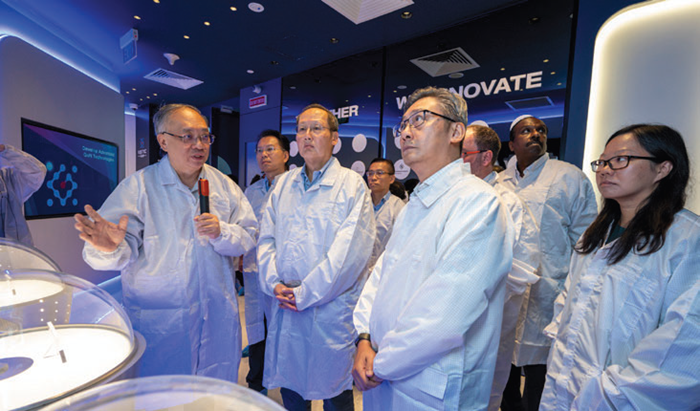
Image Credit: Oxford Instruments Plasma Technology
Supporting R&D, Regional Collaborations, and Singapore’s Semiconductor Ecosystem
Oxford Instruments’ core aim throughout this project is to collaborate closely with A*STAR, local research institutions, and industry partners to advance R&D efforts in GaN/SiC technology.
Providing advanced manufacturing tools and sharing technical expertise is key to enabling the rapid innovation and commercialization of GaN and GaN-on-SiC-based solutions.
Oxford Instruments also contributes to strengthening Singapore’s semiconductor ecosystem by enabling the broader adoption of advanced GaN and SiC manufacturing processes.
The program aims to position Singapore as a key player in the global wide bandgap (WGB) supply chain, simultaneously supporting the country's overarching goals of economic growth and technological innovation.
Powering Innovation in GaN / SiC Device Development
Oxford Instruments is also contributing to the scalability of GaN/SiC technology, enabling the implementation of high-precision, efficient production processes.
The company’s tools, like those used at the new NSTIC, support the transition of GaN / SiC devices from their research and prototyping stages through to pilot production and high-volume manufacturing. In turn, this ensures the technology can accommodate increasing global demand.
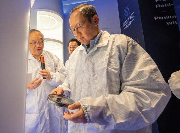
Image Credit: Oxford Instruments Plasma Technology
The company’s expertise in plasma etching, deposition, ALD, and ALE technologies is also key to enabling precise and scalable fabrication of semiconductor devices, with these tools proving essential in meeting the challenges in material interfaces and better tailoring material properties to high-performance application requirements.
Mr. Cheong Chee Hoo, Chairman of the NSTIC (GaN) Steering Committee, has stated that the NSTIC (GaN) is more than a facility. It’s a national platform for innovation and a catalyst for future technologies.
Strategic Goals and Developments
The partnership between NSTIC (GaN) and Oxford Instruments underscores Singapore’s commitment to remaining at the forefront of global semiconductor technology innovation, bringing societal and economic benefits and significant technological advances to Singapore.
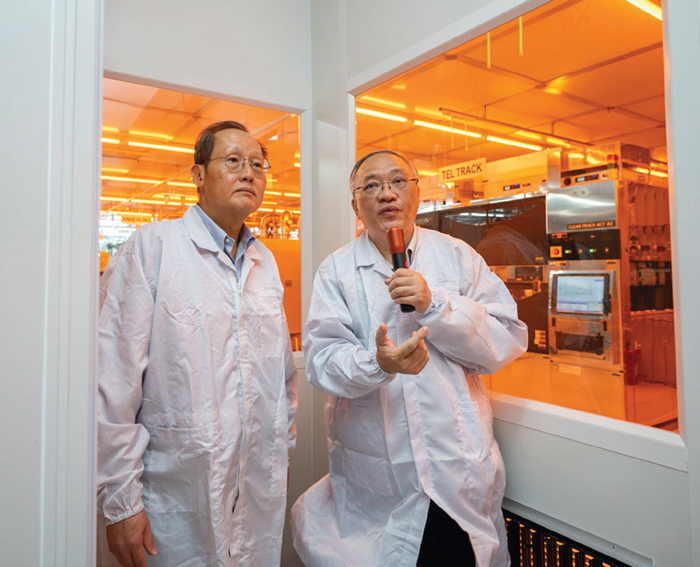
Dignitaries visiting the National Semiconductor Translation and Innovation Centre for Gallium Nitride – NSTIC (GaN) facility. Image Credit: Oxford Instruments Plasma Technology
Global Leadership in Advanced Semiconductors
Focusing on pioneering GaN technology will enable Singapore to position itself as a global leader in semiconductor innovation, improving its competitiveness and strengthening its position in the global market.
Advancing GaN Technology
GaN and GaN-on-SiC semiconductors are key to the semiconductor industry’s future due to their advanced properties, including faster performance, higher energy efficiency, and reduced size versus traditional silicon-based solutions.
Collaborative Effort and an Improved R&D Ecosystem
The initiative will encourage collaboration among research institutions, industry partners, and government agencies to expedite the innovation, prototyping, and commercialization of GaN/SiC technologies.
Long-Term Goals
The NSTIC (GaN) is working to reinforce Singapore’s semiconductor ecosystem by driving R&D, fostering the development of local talent, and attracting global partnerships.
Economic Impact
Semiconductors continue to be a cornerstone of Singapore's economy, accounting for 6 % of GDP and supporting approximately 35,000 skilled jobs across design, R&D, and advanced manufacturing.
It is expected that the GaN Centre will contribute to the country's ongoing growth in high-value manufacturing and innovation in rapidly growing markets such as the automotive, telecommunications, and clean energy sectors.
New Job Opportunities
The initiative will create jobs in engineering, manufacturing, R&D, and other high-skill areas. This will also include workforce development programs to upskill local talent, ensuring that Singapore remains globally competitive in its semiconductor workforce.
Attracting Investment
The GaN Centre is expected to draw start-ups, multinational corporations, and research institutions to Singapore by fostering a strong research and development ecosystem. This will further strengthen the country’s status as a semiconductor hub.
Applications Across Industries
The superior efficiency, speed, and compact size of GaN/SiC technology will drive technological advancements across multiple sectors, enabling innovations in industries such as healthcare, clean energy, telecommunications, and automotive applications.
Enabling Greener Technologies
GaN / SiC semiconductors are extremely energy-efficient, meaning that they are ideally suited to use in electric vehicles, renewable energy applications, and power electronics. These capabilities align with Singapore's sustainability goals and worldwide efforts to lower carbon emissions.
Supporting a Low-Carbon Economy
Adopting GaN/SiC technology for energy-efficient applications will support industries’ efforts to reduce energy consumption, thereby furthering Singapore’s green transformation agenda.
Integration Into the Global Supply Chain
Singapore strengthens its role in the global semiconductor supply chain by advancing GaN / SiC technologies, helping to ensure the country’s resilience and leadership in a rapidly evolving industry.
Expanding Market Reach
The GaN Center initiative will allow Singapore-based companies to access high-growth global markets for GaN / SiC applications, including autonomous vehicles, 5G infrastructure, and advanced medical devices.
Summary
Oxford Instruments is proud to have undertaken a key role in this transformative project, which will deliver technological leadership, energy efficiency, economic growth, job creation, and sustainability benefits to Singapore.
Acknowledgments
Produced from materials originally authored by Matt Kelly from Oxford Instruments Plasma Technology.

This information has been sourced, reviewed, and adapted from materials provided by Oxford Instruments Plasma Technology.
For more information on this source, please visit Oxford Instruments Plasma Technology.