Oxford Instruments’ new cleanroom facility perfectly demonstrates the precision and flexibility of its plasma processing solutions in both research and production settings.
This new 1200 sqm facility features 50 % more demo systems in a purpose-built space designed to offer a controlled environment suitable for tailored demonstrations, allowing the company’s customers to observe and assess the capabilities of plasma process solutions under ideal conditions.
The ISO 6/5 cleanroom replicates the quality and stability of production environments by offering a contamination-free setting. This allows the repeatability and accuracy of Oxford Instruments’ advanced plasma processes to be optimally demonstrated.
Maintaining stable operating conditions also allows the facility to deliver consistent, reliable results, making it ideally suited for evaluating a wide range of etch, deposition, atomic layer deposition (ALD), and atomic layer etch (ALE) applications at up to 200 mm wafer size.
All tools within the cleanroom undergo regular health checks, standard checks, and routine maintenance to ensure optimal performance. These checks are performed efficiently using the company’s PTIO user interface, with protocols designed to minimize downtime and ensure that all equipment operates consistently and at peak efficiency.
These protocols and checks ensure that demonstrations provide accurate and dependable outcomes, confidently reflecting the robustness of the innovative processes being assessed.
The facility also incorporates JMP software and other data-driven tools developed to help design experiments, analyze trends, and evaluate process repeatability. These analytical tools provide deeper insights into the instruments’ capabilities, optimizing processes, and identifying tailored solutions that meet the needs of specific applications.
The cleanroom supports a thorough, evidence-based approach to plasma processing demonstrations, using statistical and experimental data.
Cleanroom operations are also designed to be flexible, accommodating both research and volume production users’ requirements. This degree of flexibility ensures that each demonstration’s outcomes are relevant to customer goals.
This focused, data-rich environment is ideally suited to evaluating Oxford Instruments’ advanced plasma processing capabilities. Its combination of optimally maintained tools, data-driven insights, controlled conditions, and expert guidance allows the facility to offer a reliable platform for exploring the potential of Plasma Technology's processing solutions across a wide range of applications.
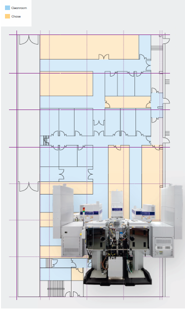
Image Credit: Oxford Instruments Plasma Technology
Plasma Process Technology Systems
ICP
Inductively Coupled Plasma and Reactive Ion Etch offers wide-ranging etch capability, supporting markets including microLEDs and metalenses, GaAs & InP optoelectronics, and SiC & GaN power/RF.
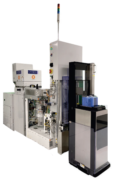
Image Credit: Oxford Instruments Plasma Technology
ALD Production
An Atomic Layer Deposition volume-manufacturing high-rate system supports device fabrication for compound semiconductor production markets, such as GaN power.
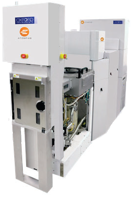
Image Credit: Oxford Instruments Plasma Technology
IBE/IBD
Ion Beam Etch and Ion Beam Deposition offer slanted etch and deposition with specialist capabilities suitable for SiC-based applications, particularly in the rapidly expanding augmented reality market.
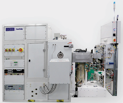
Image Credit: Oxford Instruments Plasma Technology
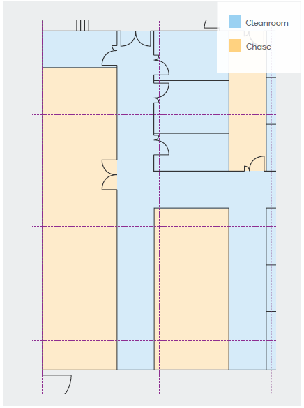
Image Credit: Oxford Instruments Plasma Technology
Nano CVD/PECVD
Chemical Vapor Deposition and Plasma Enhanced Chemical Vapor Deposition systems are well-suited to the growth of 1D/2D heterostructures and nanomaterials.
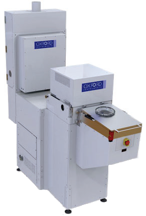
Image Credit: Oxford Instruments Plasma Technology
ALD Research and Pilot Production
Atomic Layer Deposition systems combining high rate with additional hardware flexibility are ideally suited to use in quantum ALD applications and ALD research projects, where low rate has historically been a limiting factor.
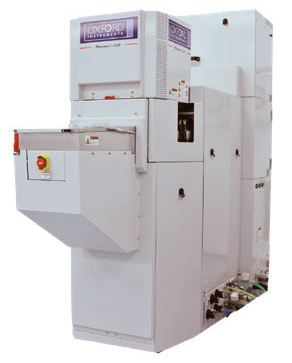
Image Credit: Oxford Instruments Plasma Technology
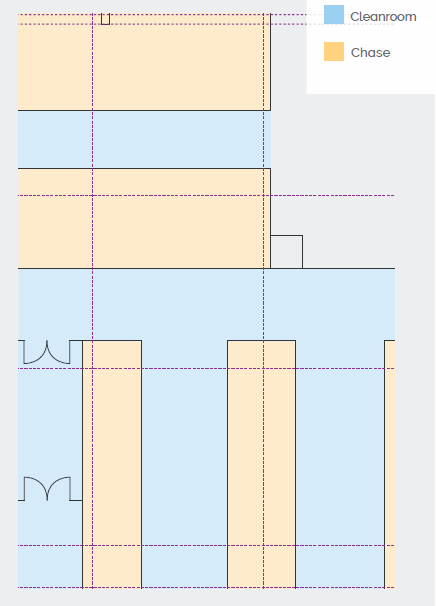
Image Credit: Oxford Instruments Plasma Technology
ICPCVD and PECVD
Inductively Coupled Plasma Chemical Vapor Deposition and Plasma Enhanced Chemical Vapor Deposition offers superior quality deposition with precise control of film properties at both high and low temperatures. These capabilities are key to preventing thermally induced damage in a wide range of research and production applications.
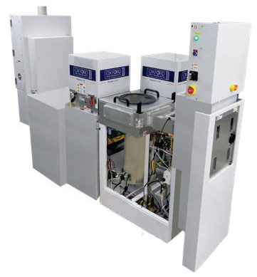
Image Credit: Oxford Instruments Plasma Technology
DRIE and RIE
Deep Reactive Ion Etch for high-rate Bosch deep silicon etch applications are also available, with an additional post-through silicon via (TSV) plasma polishing process that can remove scallops. This technology enables superconducting TSVs when combined with ALD for TSV coating.
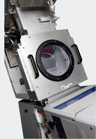
Image Credit: Oxford Instruments Plasma Technology
One of the Most Advanced Semiconductor Metrology Labs in Europe
Metrology is a key component in Oxford Instruments Plasma Technology’s workflow, supporting the inspection and measurement of both structures fabricated within the newly developed state-of-the-art cleanroom and customer samples.
These capabilities underpin the maintenance of high-quality standards, expediting research and development, and facilitating the fabrication of increasingly precise and advanced structures.
The company’s expanded new facility has also allowed the acquisition of advanced instrumentation, considerably extending its metrology capabilities. For instance, two new high-resolution scanning electron microscopy (SEM) systems were recently installed, each fitted with advanced detectors and tools to further the lab’s capabilities.
Focused ion beam (FIB) enables precise sample milling for cross-sectional analysis and the preparation of transmission electron microscopy (TEM) lamellae.
It is then possible to lift out these lamellae with an Omniprobe before they are analyzed using the in-built STEM detectors. The Ultim Extreme Infinity detector can also be used for high-sensitivity compositional analysis.
The cleanroom is built on raised flooring, with all metrological equipment located on a thick concrete base to minimize vibrations.
SEMs, atomic force microscopy (AFM) systems, and other equipment particularly sensitive to vibrations are also mounted on Quiet Islands that incorporate active vibration cancellation technology. This configuration ensures optimal accuracy and resolution with no interference from environmental noise.
Dr. Kate Stokes recently joined the Plasma Technology team based in Oxford Instruments’ new metrology lab, with her expertise helping to improve the lab’s capacity for correlative microscopy.
This is a key capability in terms of cross-referencing sample analysis techniques in order to gain deeper insights into material properties and characteristics. Dr. Stokes cross-trained on Oxford Instruments' diverse range of metrology techniques, from detectors in High Wycombe to AFMs in Santa Barbara, bridging materials analysis and plasma processing.
This combination of highly specialized fabrication tools and advanced metrology equipment results in a seamless customer demo workflow that delivers critical 'full-story' analysis.
Semiconductor Metrology Equipment from Oxford Instruments Group
A range of metrology equipment is available in the new facility.
Jupiter XR AFM
The Jupiter XR AFM offers rapid, high-resolution mapping of mechanical, topographic, and electrical properties across large-area samples, supporting sample sizes up to 200 mm.
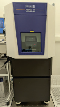
Image Credit: Oxford Instruments Plasma Technology
Zeiss Gemini560 with Oxford Instruments Detectors
The Zeiss Gemini560 offers advanced imaging capabilities. Sub-nanometer resolution is possible at low accelerating voltages, and the instrument includes a built-in STEM detector and Sense backscatter detector (BSD).
It features an Ultim Max 65 Infinity EDS detector suitable for compositional mapping, while the Ultim Extreme Infinity is available for more challenging EDS analysis, for instance, the characterization of samples at short working distances and low kV.
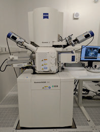
Image Credit: Oxford Instruments Plasma Technology
Alpha300 Semiconductor Edition
The WiTec Alpha300 Semiconductor Edition is a confocal Raman and photoluminescence (PL) microscope specifically designed to enable chemical imaging of semiconducting samples.
Its vibration damping, extended-range scanning stage, and active focus stabilization capabilities enable automated analysis of wafers up to 300 mm.
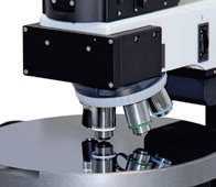
Image Credit: Oxford Instruments Plasma Technology
Zeiss Gemini 350 XB with Oxford Instruments Detectors
The Zeiss Gemini350 XB is an extremely versatile platform offering a combination of high-resolution SEM and FIB capabilities that enable simultaneous surface imaging and precision milling, as well as material deposition via a gas injection system (GIS).
The instrument is fitted with a Symmetry S3 EBSD detector suitable for rapid and accurate crystallographic characterization. An Omniprobe 400 nanomanipulator enables the lift-out of FIB-prepared TEM samples while an Ultim Max 170 Infinity EDS detector delivers detailed compositional analysis.
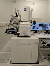
Image Credit: Oxford Instruments Plasma Technology
Hitachi S-4800
The Hitachi S-4800 SEM is a reliable tool designed for high-resolution surface imaging. It is equipped with a Delmic Sparc Spectral cathodoluminescence detector and is especially well suited to routine inspection and general-purpose analysis.
Woollam Ellipsometer M-2000
The Woollam M-2000 is a spectroscopic ellipsometer able to extract thickness and index of refraction data for semi-transparent and transparent thin films or coatings. It also offers fully automated sample alignment capabilities with stage tip/tilt.
KLA F50
The KLA F50 leverages spectral reflectance techniques to measure the thickness of thin films with high accuracy.
KLA Tencor P17
The KLA Tencor P17 benchtop stylus profilometer can be used to perform measurements such as texture, form, and step heights, as well as to detect the presence of defects and stresses.
KLA-Tencor 6420 Surfscan
The KLA-Tencor 6420 Surfscan employs high-resolution optical imaging to detect and categorize any defects present on semiconductor wafers.
Eumetrys YPI-MX
The Eumetrys YPI-MX utilizes high-resolution laser scanning in order to perform surface inspection and particle detection across a diverse array of materials, including semi-transparent, transparent, and bowed wafers.
Toho-4PP
The Toho 4-point probe offers accurate and reproducible sheet resistivity and film thickness measurements. It ensures high-precision electrical characterization of thin films and semiconductor materials through two current-supplying and two voltage-sensing probes.
Sensofar PLu-Neox
The Sensofar PLu-Neox optical profiler offers multimodal surface analysis via a combination of phase-shift and vertical-scanning interferometry, confocal scanning, and spectroscopic reflectometry. The instrument’s versatility allows the detailed characterization of both thin film properties and surface morphology.
Toho FLX-2320-S
The Toho FLX-2320-S thin-film stress measurement instrument can be used to calculate film stress by measuring the change in the radius of a substrate’s curvature caused by the deposition of a thin film on the substrate.
The tool is fitted with a hot chuck design to enable the study of temperature- and annealing-induced effects on film stress.
Olympus Microscope BX51
The Olympus Microscope BX51 has the capacity to perform dark-field, bright-field, fluorescence, and polarization microscopy, making it ideally suited to sample observation and analysis.
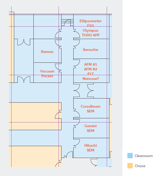
Image Credit: Oxford Instruments Plasma Technology
Acknowledgments
Produced from materials originally authored by Dr. Owain Thomas from Oxford Instruments Plasma Technology.

This information has been sourced, reviewed, and adapted from materials provided by Oxford Instruments Plasma Technology.
For more information on this source, please visit Oxford Instruments Plasma Technology.