Silicon carbide MOSFETs are beginning to replace their MOSFET and IGBT silicon counterparts in a range of high-volume power applications.
SiC’s market share continues to grow as the industry works through the remaining barriers to large-scale adoption. These include cutting chip costs, reducing defects that affect die size and yield, addressing concerns over reliability and ruggedness, and equipping engineers to use SiC in power converters.
SiC MOSFET technology has made considerable progress via multiple generations’ worth of enhancements since its initial commercial introduction in 2011, but the poor SiC/SiO2 gate interface quality continues to show significant room for improvement, attracting rigorous research.
The silicon gate-oxide MOSFET interface retains between 30 % and 60 % of the 1400 cm2/Vs bulk electron mobility, while the SiC-oxide interface retains between 3 % and 5 % of the bulk 800 cm2/Vs value.
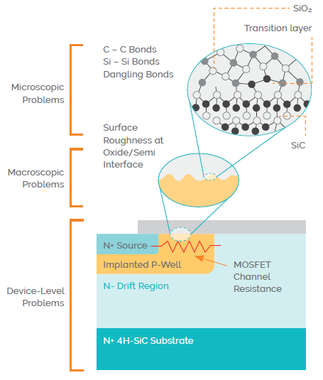
Figure 1. Trapping of electrons in interface states (DIT) degrades mobility and causes threshold voltage instability. Image Credit: Prof. J. Cooper
Macroscopic issues, such as surface roughness at the SiC-oxide interface, and microscopic problems, such as the significant density of C-C, Si-Si, and dangling bonds (Figure 1), have a deleterious effect on SiC MOSFET reliability and performance.
Trapping electrons in interface states (DIT) degrades mobility, increasing on-state resistance and conduction losses.
Trapping electrons also leads to ‘threshold voltage’ instability, creating a further concern around reliability. For example, a positive shift in threshold voltage increases resistance, while a negative shift makes the MOSFET vulnerable to involuntary turn-on with potentially disastrous consequences.
The ‘standard’ process of gate thermal oxidation starts with inserting the sample in flowing O2 at low temperature to grow a thin oxide layer and prevent loss of silicon from the SiC surface.
Dry or wet oxidation at approximately 1200 °C is used to form the gate oxide, with a further argon anneal used to remove carbon from the bulk oxide. This process is followed by a low-temperature oxidation to minimize the transition layer, then a post-oxidation anneal in nitric oxide (NO) used to passivate the interface states.
The latter of these process steps represented a major breakthrough in enabling commercial SiC MOSFET manufacture. Work is ongoing to achieve improvements in the SiC/oxide interface. However, progress in this area offers significant pay-off in terms of enhanced reliability and performance.
The formation of high-quality conformal dielectrics on the SiC surface via atomic layer deposition (ALD) represents a promising means of addressing the poor SiC/oxide interface.
Several semiconductor equipment manufacturers, including Oxford Instruments (a Power America member), offer ALD tools and optimized recipes designed to form SiC/dielectric interfaces with a low density of deleterious interface states.
ALD of materials with high dielectric constants can also reduce the impact of high SiC electric fields on the gate dielectric, thereby enabling more reliable MOSFET operation.
MOSFETs rated at 1200 V and below are beginning to achieve economies of scale due to the mass commercialization of electric vehicles and switching power supplies. Channel resistance remains the largest contributor to overall resistance at these voltage ratings, after the ‘standard industry’ thinning of the substrate from 350 µm to 100 µm.
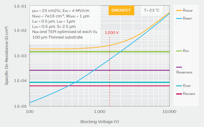
Figure 2. Specific on-state MOSFET resistance component contributions as a function of blocking voltage, for a substrate thinned to 100 μm. Below 1200 V, the channel resistance is the largest contributor to the total resistance. Image Credit: Prof. J. Cooper
Figure 2 illustrates the different MOSFET resistance components as a function of blocking voltage.
A few approaches to minimizing channel resistance exist, but they must be balanced against trade-offs such as MOSFET robustness under fault conditions.
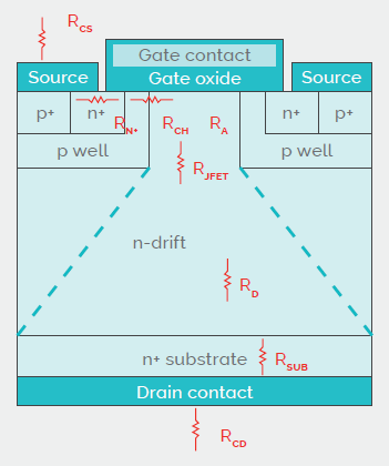
Figure 3. Schematic of planar MOSFET. Electron conduction is through a lateral channel and a vertical JFET region situated between the p-wells. Image Credit: Oxford Instruments Plasma Technology
Planar and trench MOSFETs are commercially available at 1200 V and below, with the latter exploiting the vertical channel configuration in order to reduce channel resistance. Figure 3 shows a planar MOSFET with its associated resistance elements. Its total resistance is calculated by the following equation:
RON,D = RCS + RN+ + RCH + RA + RJFET + RD + RSUB + RCD
Electron conduction in a planar MOSFET takes place via a lateral channel and a vertical JFET region located between the MOSFET p-wells. Figure 4 shows a trench MOSFET with its associated resistance elements.
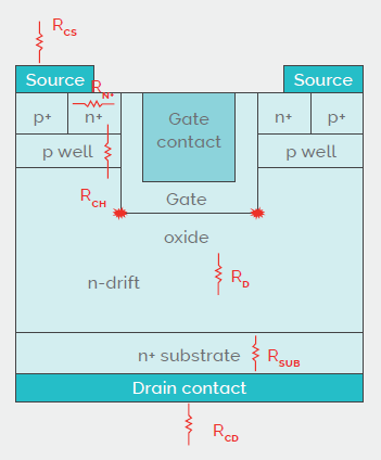
Figure 4. Schematic of trench MOSFET. Electron conduction is through a vertical channel. Image Credit: Oxford Instruments Plasma Technology
Electron conduction in a trench MOSFET occurs through a vertical channel, eliminating the JFET region's on-state resistance. It is also important to note that 4H-SiC mobility is anisotropic, with higher values in the vertical direction. The vertical channel reduces the MOSFET's lateral extent on the wafer, enabling the use of a smaller pitch and, therefore, more MOSFETs per wafer.
The trench MOSFET configuration is able to reduce device resistance, but blocking-voltage capability can be lower than that of a planar MOSFET (for the same drift layer specs) as a result of crowding of the electric field at the gate oxide’s trench corners.
Specialized designs are generally used to alleviate electric-field crowding at trench edges, but they can potentially increase fabrication complexity. This adds additional requirements for producing defect-free interfaces and sidewalls with minimal roughness for high mobility, and a flat bottom with rounded corners to alleviate electric-field crowding.
Equipment manufacturers are developing tools with atomic-scale processing capabilities, such as atomic layer etching (ALE), to address these issues. ALE and similar tools minimize surface damage while producing low-defect interfaces and low-roughness sidewalls for high mobility.
Optimized ALE recipes also support trenches with good depth control, flat bottoms, and rounded corners with a radius able to reduce electrical field crowding. Followed by ALD, it is possible to deposit conformal dielectric layers with precise thickness control and low pinhole levels.
Trapping electrons in SiC/gate-oxide interface states (DIT) reduces mobility and causes ‘threshold voltage’ instability.
These characteristics have prompted semiconductor equipment manufacturers to develop ALD and ALE tool solutions can deliver conformal SiC/dielectric interfaces with a low density of interface states, along with trenches that minimize surface damage and provide low-roughness sidewalls for high mobility.
Acknowledgments
Produced from materials originally authored by Professor Victor Veliadis from PowerAmerica and NC State University.

This information has been sourced, reviewed, and adapted from materials provided by Oxford Instruments Plasma Technology.
For more information on this source, please visit Oxford Instruments Plasma Technology.