The boom in technological advancements over the last few decades continues to have a major impact on our world.
From green energy and quantum computing to healthcare and AI, technology companies continue to innovate, developing new technologies while also finding ways to accelerate existing breakthroughs.
Areas such as AI, mobile multimedia streaming, autonomous driving, the Internet of Things (IoT), and 5/6G are undergoing a technology revolution, transforming the global way of life. These changes and developments have increased demand for data center infrastructure and complex devices, while sustainable innovation has never been higher.
Data centers are now implementing 800 G to cope with the avalanche of data, with the expectation that these requirements will reach 1.6 T in the future. It is also important to remember that the energy required to produce such huge amounts of data necessitates an equally large amount of power for cooling hardware.
A study by Deloitte entitled "Powering Al" reported that data centers currently consume around 1.4 % of the world's electricity at 380 TWh, but it is anticipated that energy consumption will increase to as much as 1000 TWh by 2030.1
McKinsey has reported that there will also be a need for US$250 - 300 bn in data center infrastructure investments.2 It’s widely accepted that data center capacity must increase by 50 % solely to accommodate the data generated by new Al applications.
The significant increase in fiber-optic network traffic is prompting high volume manufacturing (HVM) datacom device fabrication facilities to manufacture increasingly higher volumes and/or higher performing devices, while ensuring that they continue to maintain reliability.
Devices that contain indium phosphide (InP) are essential for longer range data transfer, while gallium arsenide (GaAs) remains the preferred material for shorter range, rack-to-rack data transfer.
Both InP and GaAs are key to delivering > 800 G datacom capability. Oxford Instruments launched the first datacom-focused InP plasma etch production solution in the 1980s. The company continues to be the market leader in the datacom space, offering innovative, reliable HVM production solutions able to rise to the challenge of the ongoing datacom boom.
The Challenges of the Datacom Boom
Many technology booms and device ramps have already occurred, and the means of addressing their needs remains the same: automated manufacturing on increasingly larger wafer sizes, while maintaining quality.
Devices like the distributed feedback (DFB) laser have been highly beneficial for InP datacom, enabling features within the device to more efficiently convert power to light.
The formation of a clean, smooth, continuous ridge (using plasma etch) is one of the most important processes in the fabrication of DFBs, because this process confines and couples the photons into the fiber-optic cable.
The device’s light-transfer efficiency (i.e., its quality) is significantly reduced if the ridge’s geometry and surface characteristics are not ideal.
Device performance is also reduced if the feature’s base exhibits micro-trenching (a small 'v' shape at the base of the ridge). The ridge must have smooth, clean sidewalls and a base with zero (or minimal) micro-trenches to ensure maximum power-to-light conversion efficiency.
Automation is the key enabler of many device production ramps seeking to satisfy a major market boom. For example, it will not be possible to achieve the desired scalability and consistency by running smaller wafers or pieces and venting the chamber to atmospheric pressure between process runs to manually load and unload delicate substrates.
Automation provides 24/7 operation with minimal manual wafer handling. This means lower levels of breakage and surface particle defects, both of which reduce production wafer yield.
Automated robot cassette load also allows the process chamber to be maintained at low pressure, cutting venting time between runs. Not venting between runs also ensures a more consistent wafer-to-wafer chamber condition.
Process result is another vital type of consistency, beyond the need to ensure stable manufacturing processes.
Ensuring consistently repeatable process results is a fundamental requirement for any advanced manufacturing process. This means consistently stopping the process when forming the ridge in InP using a plasma etch process. This should be done using an automated endpoint solution to stop the process at the same ideal point to control depth.
Doing so controls feature geometry while protecting underlying layers within the structure, a consideration that is more challenging when a micro-trench is present.
Oxford Instruments has pioneered this type of innovative endpoint technology in compound semiconductors like InP, GaAs, and gallium nitride (GaN) for many years.
Managing ridge formation quality requirements for increasing InP device performance is key to producing the ideal feature geometry and characteristics, and this result must be reliably and consistently delivered through automated processing.
In order to scale production to satisfy the datacom market boom, it is also necessary to increase production output while maintaining quality.
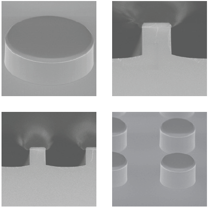
Figure 1. Automated 6-inch wafer process with a cross wafer etch uniformity of less than ± 3 %. Image Credit: Oxford Instruments Plasma Technology
It is possible to increase the number of devices produced without simply increasing the number of production runs in two key ways: by increasing the number of die (chips) per wafer, or increasing the wafer size to accommodate more dies per wafer.
There has been no major consumer-driven move toward miniaturization in datacom devices, compared to, for instance, microLEDs. Reducing the pixel size of microLEDs increases picture quality and improves the user experience.
This is key to the performance of wearable microLED devices like smartwatches, and especially to augmented reality glasses, where adoption depends on weight and comfort.
Without a consumer-driven push toward miniaturization, moving to > 6-inch wafer sizes is the clear choice for increasing die per wafer and meeting device demand for InP.
There are several technical challenges associated with producing 6-inch substrates, which are the starting material for device production. The main challenge, however, lies in maintaining ridge etch quality at 6-inch wafer size.
Hotter process temperatures (e.g., > 200 °C) have historically been used to achieve smooth, clean, low-microtrench ridge etch results. This is due to the involatile nature of the compounds given off when etching InP using standard semiconductor process gases.
This can be achieved by simply allowing the wafer temperature to increase to an uncontrolled level, because the exothermic etch processes will generate their own surface heat. This approach, however, faces reproducibility limitations and does not scale well to larger wafer sizes.
A more advanced method involves using an electrostatic chuck (ESC) to hold the wafer in place while the ESC delivers a precise amount of heat to the wafer.
Hot ESC achieves much more reliable and consistent process results, but neither hot oil nor resistively heated ESC designs have been able to achieve the mean time between failure (MTBF) required by HVM device manufacturers until recently.
Failure modes that limit MTBF can be resolved by improving materials and designs, helping to avoid high leakage current due to material breakdown, delamination of material layers, and arching of electrical components.
These failure modes typically require ESC exchange and maintenance intervention, resulting in delays and increased production costs.
Despite its process benefits, hot ESC hardware with generally low MTBF has historically posed challenges in terms of its management in production environments.
A solution to these issues has been sought for some time, prompting Oxford Instruments to launch its innovative, newly designed hot ESC. Extensive testing at HVM customer facilities producing InP optoelectronic devices has shown that this method is not inhibited by common failure modes.
The resistively heated design’s reliability has been measured by performing heat-cool cycles until component failure. This process has been significantly extended, delivering MTBF rates consistent with the needs of HVM InP device manufacturers.
Figure 1 shows the results from the company’s automated 6-inch wafer process, boasting cross-wafer uniformity of less than ± 3 %. The newly designed hot ESC can also exceed the typical upper limit of processing temperature, widening the process window in order to optimize ridge etch surface characteristics like smoothness, while also achieving micro-trench reduction by up to a factor of 10.
Oxford Instruments is positioned to continue being the key plasma etch supplier to support the datacom AI device ramp, thanks to its combination of automation at larger wafer sizes and its HVM-compatible hot ESC solution designed to maintain on-wafer result quality.
Benefits of lnP
InP is an exceptionally useful material in the development of photonic integrated circuits (PICs), which are regarded as the foundation of high-speed and low-power datacom/telecom systems.3
InP is the ideal candidate for the low-absorption windows of fiber-optic communication due to its wide, direct bandgap and desirable spectral range of 1300 nm to 1650 nm. Yole predicts the InP market will be worth around US$5.2 billion by 2029.4
Benefits of Optical Transceivers
Optical transceivers are integral components of any optical network, with the dual responsibility of both transmitting and receiving data. In the simplest of terms, transceivers condition data into light pulses to generate electrical signals.5
Lasers such as distributed-feedback (DFB) lasers are a common choice for optical transceiver production, with many HVM companies opting to use InP as the primary material for these devices.
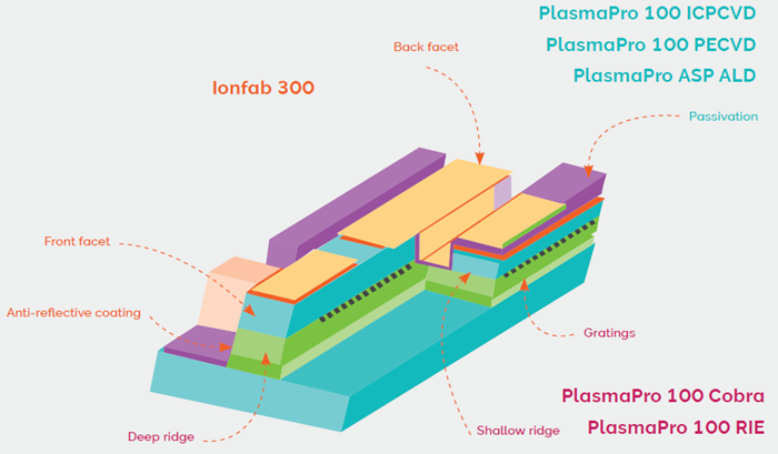
Figure 2. Schematic diagram of an InP transceiver device, and where Oxford Instruments’ modules can be used for various components of the device. Image Credit: Oxford Instruments Plasma Technology
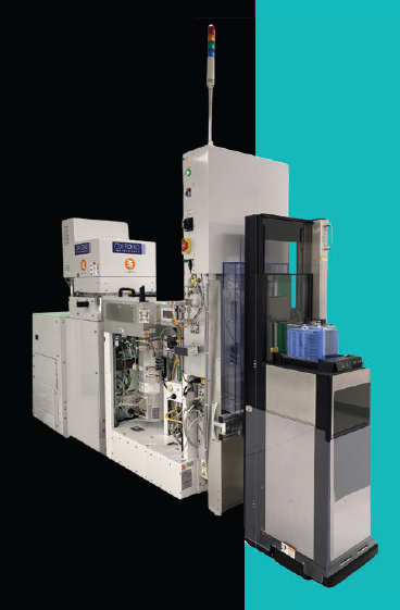
Figure 3. Oxford Instruments’ PlasmaPro100 Cobra. Image Credit: Oxford Instruments Plasma Technology
Optical transceiver production requires complex, multi-step processes that involve epitaxial deposition, masking, and plasma etching. Plasma etch is also useful in the construction of the waveguides and gratings employed in the control of laser emissions.
Oxford Instruments offers its customers InP processes with a wide choice of modules for transceiver fabrication.
Figure 2 features a diagram of an InP transceiver device, with labels highlighting the different elements where Oxford Instruments’ modules can be used.
The PlasmaPro 100 Cobra (Figure 3) is a high-precision etch module able to create accurate vertical or sloped gratings. This powerful instrument uses a hard mask and CH4/H2 gas, offering an etch rate of > 20 nm per minute and the capacity to etch features with depths of up to 100 nm.
The PlasmaPro 100 Cobra’s etch profile can be optimized for a sloped or vertical device design by changing the process gas ratio. It is also possible to achieve precise geometry and dimensions when working with critical shallow features by maintaining a slower etch rate.
Deeply etched features have the potential to limit CH4/H2 gas precision, prompting Oxford Instruments to develop an advanced hot InP plasma processing able to overcome this limitation.
This process uses a silicon dioxide/nitride hard mask at temperatures above 150 °C. A photoresist cannot withstand this level of heat. The hard mask also allows the use of other beneficial etch chemistries, including chlorine/argon.
For example, Cl readily reacts with InP to create volatile InClx. Deposition occurs if the InClx volatility is too low, while the etch undercuts the mask if this is too high.
Oxford Instruments’ process achieves optimum InClx volatility, creating accurate structures as part of a clean and repeatable process while offering an improved mean time between cleans (MTBC) and a considerable reduction in machine downtime.
Two effective endpoint detection methods are available, both of which can be fully integrated with the Cobra system.
The first method is laser interferometry, which uses the laser light reflected from the sample surface to monitor both etch depth and the etch stop layer.
The second method is optical emission spectroscopy (OES), which can detect and end the etch within an etch stop layer of -10 nm thick, monitoring plasma glow to detect changes in emission intensity at specific wavelengths, depending on etch species or etch by-products.
The process is automatically stopped once the endpoint has been reached.
References and Further Reading
- Jackson, A. (2024). An Urgent Need to Confront AI Data Centre Energy Use. (online) Data Centre Magazine. Available at: https://datacentremagazine.com/critical-environments/how-can-we-achieve-green-ai.
- Jackson, A. (2024). Global AI Boom to Triple EU Data Centre Energy Use by 2030. (online) Data Centre Magazine. Available at: https://datacentremagazine.com/data-centres/global-ai-boom-to-triple-eu-data-centre-energy-use-by-2030.
- Yan, Z., et al. (2021). A monolithic InP/SOI platform for integrated photonics. Light: Science & Applications, 10(1). DOI: 10.1038/s41377-021-00636-0. https://www.nature.com/articles/s41377-021-00636-0.
- https://www.yolegroup.com/press-release/yg-press-news-how-long-will-the-ai-trend-continue-to-fuel-the-gaas-and-inp-markets/
- Cosmo (2024). What is Optical Transceiver: A Beginner Guide (2024). (online) Optcore. Available at: https://www.optcore.net/what-is-fiber-optic-transceiver/.
Acknowledgments
Produced from materials originally authored by Dr. Emma Coleman, Dr. Ligang Deng, and Dr. Reasat Fahim from Oxford Instruments Plasma Technology.

This information has been sourced, reviewed, and adapted from materials provided by Oxford Instruments Plasma Technology.
For more information on this source, please visit Oxford Instruments Plasma Technology.