Superconducting through-silicon vias (TSVs) are central to scalable superconducting quantum computing (SQC) platforms, supporting denser integration, larger qubit arrays, and longer coherence times.
It’s essential that development aligns with the classical 2.5D - or next-generation 3D - approach if superconducting quantum devices are to achieve acceptable scale, yield, and performance.
The classical 2.5D approach involves multiple sequential etch, deposition, patterning, and other material-engineering steps. This approach has been employed extensively for many years in silicon to fabricate devices.
The primary method described here is fully compatible with current 200 mm CMOS production capabilities and is suitable for at-scale production of record-high temperature superconducting TSVs.
A significant number of superconducting quantum computing designs feature qubits and readouts on separate chips, with an interposer to connect these components.
Having the control and readout circuits on the same chip is a superior design. Here, components are directly connected by a superconductor-lined TSV through the wafer.
Limitations in established deposition techniques, such as evaporation and sputtering, have prevented meeting the required TSV density for scalable superconducting quantum computing.
Established deposition techniques cannot meet these technical requirements because they operate in a highly directional manner, limiting their ability to deposit with high conformality. Sloped or hourglass TSV shapes can be used to enable this, but this approach limits density.
It is preferable to employ vertical and straight TSV sidewalls to reduce feature pitch and accommodate the required TSV density, but it is necessary to use a non-directional deposition technique such as plasma enhanced atomic layer deposition (PEALD) to line the sidewalls with the required superconducting material.
Non-Directional, Conformal Deposition
Niobium nitride (NbN) is an ideal material choice for superconducting quantum applications due to its superior Tc, particularly when used in above dilution refrigerator applications such as superconducting neuromorphic computing, quantum computing with integrated photonics, single flux quantum logic circuits, and superconducting nanowire single photon detector (SNSPD) arrays.
It is possible to deposit niobium nitride via PEALD, an extremely precise, self-limiting deposition technique that delivers high-quality, ultra-conformal, pinhole-free, uniform coatings with precise thickness control, compared with conventional PVD and CVD techniques.
This advanced deposition technique is used across a range of applications and, more recently, in production fabs. It allows a wide variety of materials to be grown with high film quality at CMOS-compatible processing temperatures.
PEALD’s directionality can also be closely manipulated with bias control, allowing conformal films to be deposited on vertical sidewalls, even in deeply etched TSVs.
The Challenge of Vertical TSVs for Quantum Applications
The Bosch process is the most common approach to creating vertical TSVs, but the scalloped roughness associated with it makes conformal, continuous TSV lining relatively challenging, even with PEALD.
Post-etch wet treatment to reduce the roughness is possible, but often not feasible or desirable in superconducting quantum applications, due to material incompatibilities.
The TSV can also be created via zero-scallop cryogenic etch, an alternate method that does not require post-etch smoothing treatment. This method requires a hard mask as opposed to the photoresist mask available for the development project outlined here.
The Bosch process was used to create the > 300 µm deep TSVs in this development work, leveraging its high rate and CMOS compatibility. A dry plasma etch technique was also utilized to reduce the interface roughness.
Interface optimization techniques can be categorized into polishing (for example, the removal of surface and subsurface or roughness removal), activation (for example, wafer bonding), and surface modification (for example, the removal of native oxides and the filling of nitrogen vacancies that block electron flow).
A post-etch dry TSV Plasma Polish process was utilized in this work in order to provide a smooth interface ready for deposition, and to ensure the creation of a high quality, continuous PEALD superconducting TSV liner.
TSV Polish Process Results
Three conformality results are shown. They feature the following samples:
- A-1: A sample without TSV Plasma Polish and 100 nm PEALD NbN deposition.
- A-2: A sample with TSV Plasma Polish and 100 nm PEALD NbN deposition.
- B: A sample with etch down to the oxide stop layer, with TSV Plasma Polish, the oxide layer removed, and PEALD processing on top (50 nm) and bottom (50 nm) with the wafer flipped over between processes.
Superconductivity Results for Sample B
It was observed that the in-plane portion of the film became superconducting first, at around 13.9 K, with Tc gradually decreasing through the depth of the TSV until the entire film was superconducting at approximately 10.7 K.
The diagrams highlight the superconducting film sections (in red) or resistive sections (in yellow) at specific temperatures. Results from a control sample are also included for comparison. This sample features a 30 nm NbN surface, illustrating an ideal superconductive result.
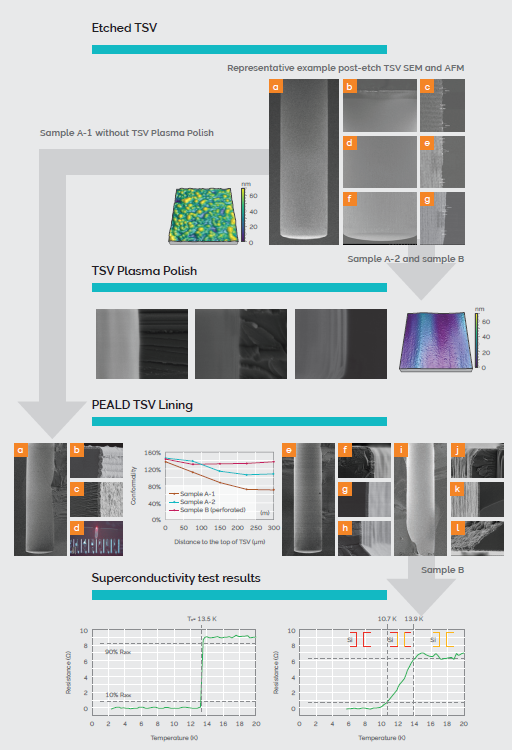
Image Credit: Oxford Instruments Plasma Technology
TSV Sidewall Preparation and Measurement
Atomic force microscopy (AFM) is a non-destructive, probe-based, mechanical surface characterization technique that involves scanning a sharp stylus, typically referred to as an AFM probe or AFM tip, over the surface of interest.
AFM generates three-dimensional, high-resolution (a fraction of a nanometer) topographic images of surfaces. AFM can measure surface roughness, critical dimensions, and samples’ electrical, thermal, and mechanical properties.
The AFM uses optical beam detection to quantify the interaction between the AFM tip and the sample. The AFM tip is mounted on a cantilever, which deflects when the tip interacts with the sample. These deflections are monitored by reflecting a laser from the back of that cantilever into a detector.
AFM offers several advantages over other surface characterization techniques, most notably its unmatched three-dimensional spatial resolution and the quantitative nature of the data acquired.
It is important to prepare the sample so as to expose the sidewall (the area of interest) when performing measurements of TSVs’ roughness or any sidewall roughness measurement.
Measuring TSVs’ surface roughness in this work involved first cleaving the sample along the vias' array (a), then rotating the sample so that the TSV interior was facing up (b). Next, the sample was aligned with the AFM probe (c) to ensure that the area of interest was visible in the AFM optics (d).
Two TSV samples were imaged, and the data compared: one before (e) and one after (f) TSV Plasma Polish.
Before smoothing, the TSV displayed a rough topography with some features reaching 70 nm in height. After smoothing, the TSV was far more uniform with a lower feature height variation below 30 nm.
Both samples were imaged with the same AFM probe (Titan 300) in order to minimize experimental variability, with the areas compared limited to 1 µm2.
The AR Maps software (included with the Jupiter XR AFM) was used to analyze surface roughness data. The ISO 25178 standard (also included in the software) was used to calculate the root-mean-square-height (Sq) of each.
Before smoothing (e), the Sq value was 12.9 nm versus the post-smoothing surface (f), where the Sq was 6.5 nm. These values confirm that the smoothing process decreased the TSV sidewall's surface roughness by around 50 %.
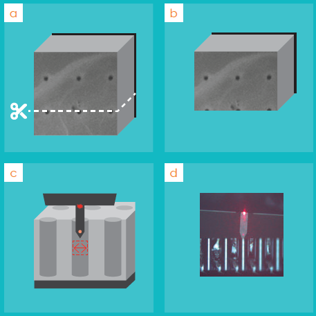
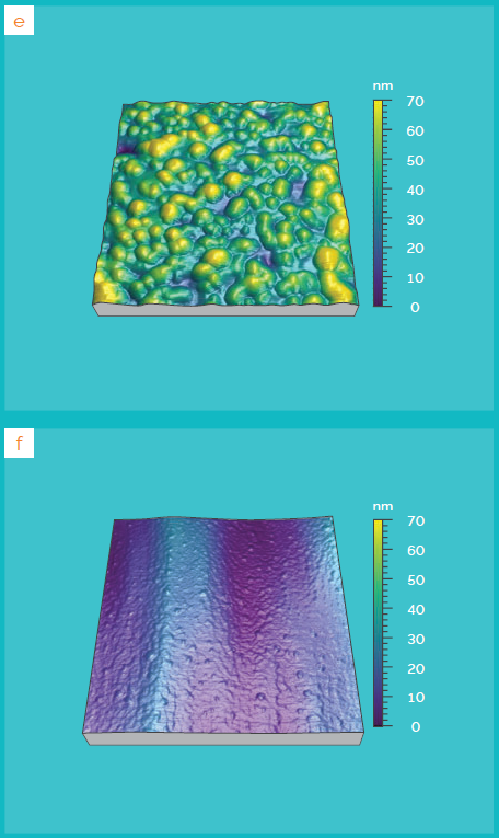
Image Credit: Oxford Instruments Plasma Technology
Conclusion
Bosch-typical scallop roughness is a limiting factor in achieving high conformality and continuity ALD. The conformality significantly improved after smoothing, however, highlighting the potential of TSV Plasma Polish in optimizing the TSV sidewall interface and delivering excellent conditions suitable for subsequent PEALD.
The combination of Bosch, TSV Plasma Polish, and PEALD also facilitates the fabrication of vertical, dense array superconducting TSVs. The smoothing step increased conformality from 67 to 110, with a record high Tc of 10.7 K niobium nitride TSVs.
Superconducting TSVs are required for crosstalk reduction, shielding, bias, and signaling in a diverse array of superconducting quantum device applications.
The combination of interface optimization methods and wafer-scale commercial fabrication processing presented here enables the realization of new large-scale superconducting quantum computing architectures, alongside a range of other electronic and photonic quantum devices.
Acknowledgments
Produced from materials originally authored by Dr. Zhong Ren and Dr. Marta Kocun from Oxford Instruments Plasma Technology.

This information has been sourced, reviewed, and adapted from materials provided by Oxford Instruments Plasma Technology.
For more information on this source, please visit Oxford Instruments Plasma Technology.