MicroLEDs are drawing growing attention. Measuring from around 1 µm to a few hundred microns, they can deliver higher light output, longer lifetimes, and lower power consumption than OLEDs.
With only a few challenges remaining, microLEDs have the potential to empower the next generation of displays in groundbreaking areas, including AR/VR, wearables, automotive, phones, and large displays.
The main barriers to widespread microLED adoption are cost-related, although some forecasts suggest these LEDs could reach cost parity with OLEDs’ 2024 pricing by 2026.
There are also challenges associated with the fabrication of red LEDs and with maintaining sufficient light output as dimensions continue to shrink.
The plasma etch process is used to define GaN LED mesa structures, but it is known to damage sidewalls and create non-radiative recombination (NRR) states, thereby reducing light output. This is generally quantified as external quantum efficiency (EOE).
Oxford Instruments Plasma Technology has an active program focused on developing a low-damage mesa etch that also removes damage from mesa sidewalls.
Early results have demonstrated promising increases in luminescence of bulk material, with further work planned on LED structures. Figure 1 shows the impact of isotropic ALE on the (cathodo-) luminescence of a damaged n-GaN mesa.
The mesa top is protected by the mask during the etch, showing no damage and generating a bright luminescence. There is damage in the GaN around it, which is causes low luminescence.
Figure 2 highlights how isotropic ALE treatment can be used to remove material from the top of the GaN and the sides. The resulting signal is far brighter, and the undamaged top is indistinguishable from the previously damaged backgrounds. This confirms the removal of the damaged part.
Further work is required to develop a useful process, but these findings validate the principle of etch-damage removal.
The manufacture of red-emitting LEDs represents a further challenge. The green and blue GaN-based LEDs are widely recognized for achieving EOEs close to 50 %. The record for red is < 10 %.
Red is, therefore, often made using AlGaInP, rather than the alloys of Al, In, and GaN utilized for other colors.
There is an advantage to this approach, which sees the fabrication of monolithic three-color LEDs whereby each LED element has red, green, and blue generating structures that operate simultaneously.
The basic material system is comprised of GaN and its alloys. InGaN is the most ideal candidate for red LEDs, but this is extremely challenging to manufacture and is currently at an early stage in its development.
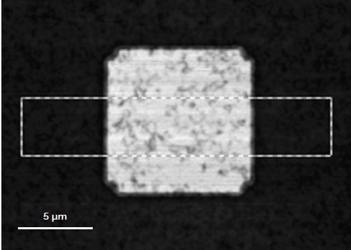
Figure 1. (Cathodo-) luminescence after mesa formation by plasma etch. Image Credit: Oxford Instruments Plasma Technology
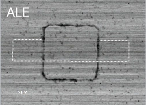
Figure 2. (Cathodo-) luminescence after additional isotropic ALE damage removal. Image Credit: Oxford Instruments Plasma Technology
Acknowledgments
Produced from materials originally authored by Dr. Andrew Newton from Oxford Instruments Plasma Technology.

This information has been sourced, reviewed, and adapted from materials provided by Oxford Instruments Plasma Technology.
For more information on this source, please visit Oxford Instruments Plasma Technology.