Demand for reliable, high-efficiency, compact power electronics has risen dramatically in recent years across a range of industries: AI data centers, electric vehicles, aerospace, renewable energy, and industrial automation.
The total power electronics market is projected to grow at a CAGR of 10 %, reaching a total market volume of $43.3 billion by 2030.1
Silicon carbide (SiC) has become recognized as the most promising, mature wide-bandgap semiconductor material able to meet this demand, offering improved physical and electrical properties compared to traditional silicon (Si).
SiC can operate at higher voltages, temperatures, and frequencies due to its wide bandgap (3.26 eV), high critical breakdown electric field (3 MV/cm), and excellent thermal conductivity. These characteristics make SiC the ideal candidate for next-generation power devices.
The material is also readily available on 8-inch wafers, with the cost proportion of SiC wafers expected to reduce from 35 % in 2021 to 24 % in 2028.1 Commercial adoption of SiC devices, most notably MOSFETs, has been slowed, however.
Several challenges in the fabrication and interface quality of these devices continue to directly impact reliability, performance, and production yield. For example, a key bottleneck in SiC device performance stems from the poor quality of the silicon dioxide (SiO2)/SiC interface.
This interface suffers from a high density of interface traps (DIT), which is 1-2 orders of magnitude higher than that of the SiO2/Si interface. High DIT results in charge trapping, high resistance, reduced channel mobility, and long-term reliability issues.
Thermal oxidation and other traditional fabrication techniques also result in carbon release at the interface, exacerbating these issues by introducing oxygen vacancies and carbon clusters.
There is a significant need for innovative approaches to overcome these limitations, prompting collaborative efforts to develop advanced deposition and processing techniques for SiC devices.
Oxford Instruments and the University of Warwick School of Engineering presented a joint research project at ICSCRM 2025 that addresses these challenges through a series of innovative solutions.
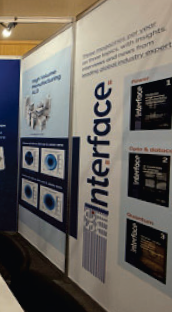
Images from ICSCRM 2025 in Busan, South Korea. Image Credit: Oxford Instruments Plasma Technology
This collaborative work aims to develop scalable and commercially viable processes for SiC-based power device fabrication by combining industry-leading expertise in atomic layer deposition (ALD), atomic layer etching (ALE), plasma processing, and advanced characterization methods.
The research is focused on enhancing the SiO2/SiC interface, exploring means of optimizing trench filling for superjunction (SJ) devices, and reducing subsurface defects in SiC substrates.
This work leverages ALE and ALD as complementary techniques. ALE offers precise control over surface conditioning, selectively terminating the SiC surface with desired elemental species to reduce DIT and enhance threshold voltage control.
ALD offers a chemistry-based approach to depositing oxide layers with minimal defects and high conformity. ALD minimizes interface traps and ensures uniform deposition across complex geometries by avoiding the carbon release typically associated with thermal oxidation.
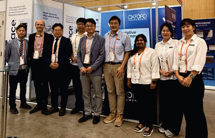
Images from ICSCRM 2025 in Busan, South Korea. Image Credit: Oxford Instruments Plasma Technology
Post-deposition annealing (PDA) at high temperatures in controlled gas environments further improves SiO2/SiC interface quality.
The scalability of these processes for commercial adoption is a further area of focus, with high-rate ALD systems like Oxford Instruments’ PlasmaPro ASP highlighting the potential of integrating advanced deposition techniques into foundry processes.
These systems facilitate high-throughput manufacturing while maintaining the precision and dielectric quality required for SiC device fabrication.
This research provides a roadmap for deposition process optimization that is suitable for use with a range of device designs and performance requirements, achieving this by systematically studying the impact of process conditions, like deposition temperatures, gas compositions, and cycle times.
This collaborative project also relies on advanced characterization tools to evaluate and fine-tune developed processes. Techniques such as atomic force microscopy (AFM) and electron backscatter diffraction (EBSD) provide detailed insights into interface trap densities, subsurface defects, and bonding environments at the SiO2/SiC interface.
X-ray photoelectron spectroscopy (XPS) and other novel characterization methods, such as time-of-flight elastic-recoil detection (ToF-ERD) provide useful information on the atomistic distribution within the oxide and the chemical bonding environment at the interface.
These measurements validate improvements achieved via ALE, ALD, and PDA while also guiding further refinements to the fabrication process by highlighting the physical mechanisms underlying improvements in device performance.
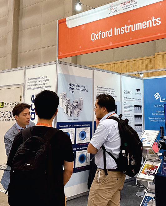
Images from ICSCRM 2025 in Busan, South Korea. Image Credit: Oxford Instruments Plasma Technology
Unlocking the Full Potential of SiC
This innovative co-development and collaboration between Oxford Instruments and the University of Warwick has the potential to overcome the challenges associated with SiC device fabrication.
This body of work showcases solutions for producing high-performance SiC devices with improved reliability and efficiency through the development of innovative deposition, surface treatment, and characterization techniques.
The results highlight the potential of advanced processes, such as ALD or ALE, combined with scalable manufacturing solutions to unlock the full potential of SiC in power electronics.
These developments are expected to play a key role in reducing energy losses, driving innovation, and facilitating the widespread adoption of SiC technology across an array of industries.
References and Further Reading
- Yole Intelligence (2024) Status of the Power Electronics Industry: Growth, challenges and the road ahead for SiC technology. Available at: https://www.yolegroup.com/strategy-insights/power-electronics-growth-challenges-and-the-road-ahead-for-sic-technology/.
Acknowledgments
Produced from materials originally authored by Dr. Arne Benjamin Renz from the University of Warwick's School of Engineering.

This information has been sourced, reviewed, and adapted from materials provided by Oxford Instruments Plasma Technology.
For more information on this source, please visit Oxford Instruments Plasma Technology.