A recent interview with Professor Paul Hurley, Head of the Nanoelectronic Materials and Devices Group at Tyndall National Institute, Research Professor at University College Cork (UCC), and Meta's Industrial Chair in Semiconductor Technologies at Tyndall and UCC for the multi-year augmented reality (AR) research program, saw Professor Hurley showcase both his technical expertise and his gift for storytelling.
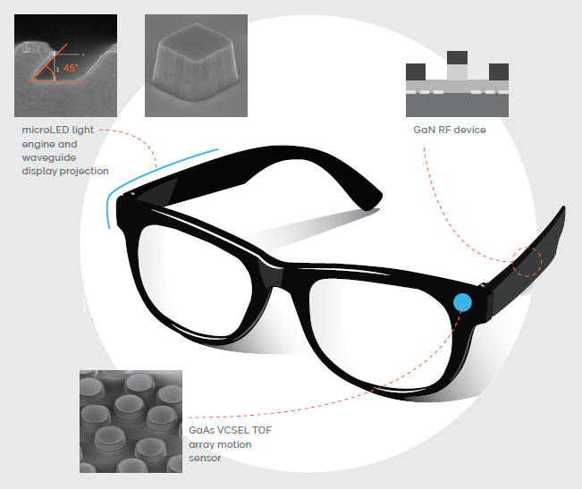
Image Credit: Oxford Instruments Plasma Technology
The interview took readers from the first transistor to today’s next-generation technologies, while showing how collaboration across scientific disciplines can drive innovation. By combining their expertise, researchers can apply material properties in new and promising ways.
This is certainly the case for silicon carbide (SiC), with this beneficial wide bandgap semiconductor becoming synonymous with high-power electronics due to its significantly higher breakdown field and improved thermal conductivity in comparison to pure silicon.
SiC’s properties are seeing it become increasingly commonplace in industrial applications, including AI data centers, green energy, electric vehicles, and aerospace technologies.
Technical challenges still exist, including achieving a reduction in interface trap density, the stabilization of threshold voltage, and safeguarding reliable longevity in extreme conditions. These challenges are being actively addressed by power device specialists, however.
Augmented reality (AR) is one SiC application that is not limited by electron-centric considerations, and the market appears to be centering on SiC as the material of choice for confining and affecting photons.
The Cork-based Meta project that Professor Hurley is currently chairing is a single piece of a larger, multifaceted initiative pursued by Meta in the field of augmented reality devices. The advancement of SiC waveguides is another part of this major undertaking.
In 2024, Meta unveiled its Orion AR glasses with SiC waveguides after many years of experimentation. This represented a major technology breakthrough, with SiC's high refractive index increasing the field of view (FOV) and improving the immersive user experience versus previously employed waveguide materials.
SiC is also lightweight, robust, and resistant to damage – all important qualities in the development of AR glasses that are comfortable enough to wear for long periods.
Major challenges in developing high-quality SiC waveguides include achieving ultra-low footing, sidewall smoothness, precise trench features, and consistent sidewall angle control and uniformity.
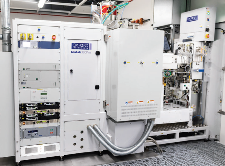
Image Credit: Oxford Instruments Plasma Technology
Oxford Instruments is currently developing advanced slanted grating etch solutions using its ion beam etch (IBE) technology, and trench and plasma polish solutions designed for use in the SiC power sector.
The SiC power electronics market is reducing large-scale wafer production costs and advancing fabrication techniques, meaning that these developments have already directly benefited the SiC AR market by making high-quality optical-grade SiC commercially viable and more accessible for waveguide applications.
Production is still in early stages, but suppliers around the world are developing optical-grade SiC, with some suppliers advancing from 4 to 8-inch wafer production and even exploring 12-inch wafers for improved economies of scale.
The adoption of SiC waveguides represents a major optical breakthrough, combining an expansive FOV with exceptional display clarity that pushes the boundaries of immersive augmented reality.
Early adopters will be excited by this increasingly clear pathway from innovation to mainstream uptake, ushering in a new era of AR experiences powered by SiC waveguides.
The Ionfab ion beam etch technology used in the production of these waveguides offers a range of benefits, including exceptional process uniformity, cost-effective operation, and suitability for both R&D and production.
It also offers uniform etching features, using a substrate shutter to cover or partially cover the material, controlling ion beam exposure, and compensating for uneven plasma exposure due to the angled stage. This can also be adjusted during the etching process.
A patented grid and plasma source feature a specialized design able to accommodate an angled stage, while reactive gas capabilities also enable improved mask selectivity.
This method also offers wafer handling options for single wafer loadlock or cassette-to-cassette automated handling.
Acknowledgments
Produced from materials originally authored by Dr. Emma Coleman from Oxford Instruments Plasma Technology.

This information has been sourced, reviewed, and adapted from materials provided by Oxford Instruments Plasma Technology.
For more information on this source, please visit Oxford Instruments Plasma Technology.