Photo-induced force microscopy (PiFM) verifies what AFM topography cannot do alone: the accidental deposition of cobalt on an alternating material line region.
Visualizing area-selective deposition (ASD) of monolayers in ALD and CVD processes is a difficult task, especially when the deposited layer lacks topographic features that separate it from the surrounding area.
Chipmetrics addresses this issue with its ASD test chip, which consists of sub-100 nm alternating material lines embedded in a planar silicon surface, allowing process teams to analyze area-selective depositions using standard metrology instruments.1
Photo-induced force microscopy (PiFM) can similarly address this issue by directly visualizing nanoscale chemical changes between ALD/CVD layers using the material's infrared absorption signature.
As a result, PiFM may be leveraged to independently characterize ASD test chips to show and validate their area-selective deposition capabilities.
This article details the use of the Vista 75 AFM to measure PiFM on a cobalt (Co)-deposited ASD chip and compare it to an uncoated chip. Specifically, the aim is to see if a Co nanolayer can be found over the alternating material line region, confirming its area-selective deposition.
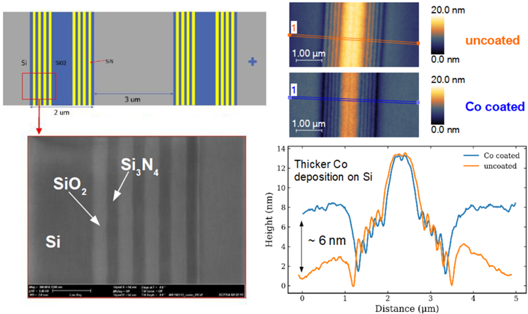
Figure 1. ASD test-chip with alternating SiO2 and Si3N4 lines on a silicon substrate (left). AFM topography (right) shows that Cobalt deposition results in a 6 nm height increase on the silicon region compared to the SiO2/Si3N4 region1. Image Credit: Molecular Vista
AFM topography photos (Figure 1) from the ASD test chip clearly indicate that cobalt deposition is not uniform. The surrounding silicon substrate region had 6 nm greater Co deposition than the alternating SiO2/Si3N4 region.
While these findings suggest a selective deposition of Co, they do not confirm whether any Co was deposited above the SiO2/Si3N4 lines.
PiFM can detect Co directly by looking for the Co-O stretch band between 500–700 cm-1. This requires a good tunable laser that can access that wavenumber range (e.g., OPO/DFG). However, even without access to that wavenumber range, the strength of photo-induced force (PiF) signals from SiO2 (Si-O stretch at 1100 cm-1) and Si3N4 (Si-N stretch at 950 cm-1) can indirectly indicate the presence of a Co layer.
A present Co layer would mask the PiF signal emanating from the underlying material's absorption bands. Therefore, by comparing the PiF intensities of a coated and uncoated sample, one may determine which regions Co was deposited in.
This indirect detection method is appropriate for situations when the accessible tunable laser (e.g., MIRcat QCL, 770–1500 cm-1) can only access wavenumbers corresponding to secondary material components of interest, not the principal one (Co in this example).
Figure 2 shows how this indirect method was used to determine the existence of a Co layer above the alternating SiO2/Si3N4 region. PiFM pictures on the uncoated ASD chip show substantial signal contrast for the Si-O stretch (1100 cm-1) and Si-N stretch (950 cm-1) absorption bands from the SiO2 and Si3N4 regions, respectively.
On Co-coated chips, the PiFM images show a lower intensity for both absorption bands, indicating that a thin Co coating must be present over the alternating line region to conceal the PiF signal.
The authors respectfully thank Mr. Thomas Werner (Chipmetrix GmbH) and Mathias Franz (Fraunhofer ENAS) for designing and supplying the ASD test chip, as well as the schematics shown in Figure 1.
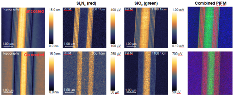
Figure 2. Topography and PiFM images at 950 cm-1 (Si3N4) and 1100 cm-1 (SiO2) wavenumbers measured on an uncoated (top) and coated (bottom) ASD test chip. An overlaid PiFM image combining the Si3N4 (red) and SiO2 (green) PiFM images is shown on the right for each case. Image Credit: Molecular Vista
References and Further Reading
- Ghaderi, Z. (2026). Chipmetrics announces new ASD-2 test chip with customizable metal–dielectric material stacks. Chipmetrics. Available at: https://chipmetrics.com/chipmetrics-announces-new-asd-2-test-chip-with-customizable-metal-dielectric-material-stacks/.
- Franz, M., et al. (2025). Low-temperature ALD of metallic cobalt using the CoCOhept precursor: Simulation-assisted process development for deposition on temperature sensitive 3D-structures. Journal of Vacuum Science & Technology A, 43(2). DOI: 10.1116/6.0004248. https://pubs.aip.org/avs/jva/article/43/2/022412/3337519/Low-temperature-ALD-of-metallic-cobalt-using-the.

This information has been sourced, reviewed, and adapted from materials provided by Molecular Vista.
For more information on this source, please visit Molecular Vista.